
 My Inquiry
 My Account


Texas Instruments UCC29002D/1
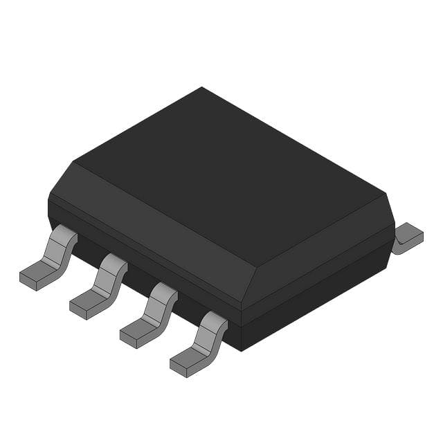
- Part No.:
- UCC29002D/1
- Manufacturer:
- Texas Instruments
- Category:
- Power Management - Specialized
- Package:
- 8-SOIC (0.154", 3.90mm Width)
- Datasheet:
-
 UCC29002D/1.pdf
- Description:
- UCC29002 ADVANCED 8-PIN LOAD SHA
- Quantity:
- Payment:

- Shipping:

Inventory:5,437
Please send an inquiry. Send us your inquiry, and we will respond immediately.
Product details
Overview
UCC29002D/1 from Texas Instruments is an advanced 8-pin BiCMOS load-share controller for N+1 redundant power systems, delivering <1% current-share error at full load, ultra-low offset (±100 µV) current-sense amplification, and Intel® SSI-compliant single-wire load-share bus operation in server and telecom DC-DC module paralleling applications.
For engineers reviewing the UCC29002D/1 datasheet, UCC29002D/1 pinout, UCC29002D/1 application, or UCC29002D/1 equivalent, key selection criteria include high-side/low-side current-sense flexibility, LS bus fault protection thresholds (VLS < 2/3×VCSO or VLS > VVDD − 0.7 V), start-up behavior (adjust current follows VEAO, not forced max), and VSSOP-8 package compatibility with remote-sense OEM power supplies.
Technical Context
The UCC29002D/1 implements automatic leader/follower architecture using a post-package-trimmed current-sense amplifier (gain ≥3, GBW = 2 MHz, CMRR ≥75 dB) and transconductance error amplifier (gM = 14 mS) to balance output currents across parallel modules. Its differential CS+/CS− inputs support GND-referenced or high-side shunt placement with 0 V to VDD common-mode range.
It features dual-stage LS bus control: a unity-gain driver with ideal-diode behavior establishes leadership dynamically, while a 15 kHz-filtered receiver monitors bus voltage (VLS) and triggers fault shutdown if VLS falls outside [2/3×VCSO, VVDD − 0.7 V]. Start-up logic differs from UCC29002/UCC39002 by omitting forced 3 V adjust input-ADJ current scales linearly with VEAO from power-on.
Key Specifications
| Parameter | Value and Actual Design Meaning |
|---|---|
| Current-share accuracy | <1% error at full load: enables precise current balancing across N+1 redundant modules without manual trimming. |
| Current-sense offset voltage | ±100 µV typ at 25°C: supports accurate low-value shunt sensing (e.g., 0.5 mΩ) with minimal power loss. |
| Input common-mode range | 0 V to VDD: allows shunt placement in either GND return or positive output rail, simplifying layout in isolated converters. |
| LS bus fault detection | VLS < 2/3×VCSO or VLS > VVDD − 0.7 V: prevents erroneous voltage adjustment during shorts to GND or supply rail. |
| Operating temperature range | –40°C to +105°C: qualified for industrial and telecom base station environments with extended thermal margin. |
| Supply voltage range | 4.575 V to 13.5 V: compatible with standard 5 V, 12 V, and intermediate bias rails; internal 14.25 V clamp protects against overvoltage. |
| Adjust sink current | 3.35–4.55 mA (–40°C to +105°C): drives external RADJ/RSENSE network to modulate feedback node voltage of connected DC-DC controller. |
Pinout & Package
UCC29002D/1 is housed in an 8-pin VSSOP package (3.00 mm × 4.90 mm), optimized for space-constrained board layouts in multi-rail power systems.
| Pin/Terminal | Circuit Role | Design Meaning |
|---|---|---|
| CS− (Pin 1) | Inverting input of current-sense amplifier | Accepts low-side or high-side shunt return; used with CS+ to generate differential sense signal; enables disable function when biased ≥0.5 V above CS+. |
| CS+ (Pin 2) | Noninverting input of current-sense amplifier | Completes differential sensing path; common-mode range includes GND and VDD, enabling flexible shunt placement without level-shifting. |
| VDD (Pin 3) | Power supply input | Bias rail (4.575–13.5 V); requires local 0.1–1 µF low-ESL capacitor; internal 14.25 V clamp limits absolute max to 15 V. |
| GND (Pin 4) | Reference ground | Common reference for all analog blocks; must connect to converter's negative sense (S−) path to avoid ground-loop errors. |
| ADJ (Pin 5) | Adjust amplifier output | Sinks current proportional to VEAO to modify feedback voltage of external DC-DC controller; zero current at leader module (VEAO ≈ 0 V). |
| EAO (Pin 6) | Error amplifier output | Transconductance output (14 mS) generating VEAO; compares VCSO (local current) to VLS (leader current); clamped to 3.5–3.8 V high-level. |
| LS (Pin 7) | Load-share bus I/O | Drives and receives single-wire bus; internal 100 kΩ input impedance; disconnects during fault/disable; leader drives bus, followers receive. |
| CSO (Pin 8) | Current-sense amplifier output | Amplified shunt voltage (gain ≥3); feeds EAO and LS driver; output swing 0–VVDD − 1.7 V ensures headroom for bus driver operation. |
Key Features
| Feature | Design Value |
|---|---|
| Intel® SSI load-share compliance | Meets specification for interoperability with industry-standard server power modules, ensuring plug-and-play redundancy. |
| Single-wire load-share bus | Reduces inter-module wiring to one trace; eliminates complex bus arbitration and enables scalable N+1 architectures up to ~10 modules (per IOUT_LS limit). |
| Ultra-low offset current-sense amplifier | ±100 µV offset trimmed post-package enables sub-milliohm shunt use without calibration, minimizing conduction loss in high-current paths. |
| LS bus short-circuit protection | Dual-window comparator detects shorts to GND or VDD and forces controller disable-prevents false voltage adjustment and system instability. |
| Start-up behavior (UCC29002-1 variant) | ADJ current tracks VEAO from power-on (no forced 3 V step), enabling smoother, lower-dV/dt engagement in sensitive distributed loads. |
Applications
| Telecom Rectifier Modules | Server PSU Redundancy |
|---|---|
|
Use Scenario: Paralleling multiple 48 V telecom rectifiers in a -48 V DC plant with remote voltage sensing. IC Role / Device Role / Timing Role: Load-share controller coordinating current distribution among independent AC/DC modules via single-wire LS bus. Use Value: Achieves <1% current imbalance across modules under full load, extending mean time between failures in carrier-grade systems. |
Use Scenario: N+1 redundant 12 V power supplies feeding CPU/GPU VRMs in rack-mounted servers. IC Role / Device Role / Timing Role: Real-time current balancing agent interfacing with TPS4005x/LM25145-based DC-DC controllers via ADJ pin feedback injection. Use Value: Eliminates need for master-slave configuration or external DACs-reduces BOM count and improves thermal derating margin. |
| Industrial PLC Power Backplanes | Medical Imaging Power Racks |
|
Use Scenario: Parallel operation of isolated 24 V DC-DC modules powering I/O modules in programmable logic controllers. IC Role / Device Role / Timing Role: High-side current sensing (shunt in +24 V rail) with GND-referenced CS+ and CS− inputs. Use Value: Maintains ±100 µV offset accuracy despite noisy industrial ground planes, ensuring stable current sharing during transient load steps. |
Use Scenario: Redundant high-current 5 V/3.3 V power racks supplying CT/MRI subsystems requiring zero-downtime operation. IC Role / Device Role / Timing Role: Leader/follower arbitration over LS bus with automatic fault isolation when one module fails open-circuit. Use Value: Enables hot-swap capability and continuous operation during field maintenance-meets IEC 60601-1 safety requirements. |
Equivalent & Alternatives
The following parts are listed as comparable options for similar load-share controller applications.
| Alternative Part | Technical Difference | Application Difference | Selection Advice |
|---|---|---|---|
| UCC29002DR | Same silicon, SOIC-8 package (4.90 mm × 6.00 mm); higher RθJA (111.9°C/W) vs. VSSOP (168.0°C/W); identical electrical specs. | Preferred where board real estate permits larger footprint and thermal management uses heatsinking or airflow. | Select UCC29002DR for legacy SOIC-compatible designs or when VSSOP assembly is unavailable. |
| UCC39002DGKR | Same functional block diagram but rated for 0°C to +70°C only; lacks –40°C startup guarantee; identical pinout and interface. | Suitable for commercial-grade telecom access equipment or indoor server peripherals with controlled ambient. | Choose UCC39002DGKR only when industrial temperature range is not required-lower cost, same layout. |
Compared with UCC29002D/1, UCC29002DR trades thermal performance for mechanical compatibility, while UCC39002DGKR sacrifices extended temperature operation for cost reduction-neither offers pin-to-pin replacement without verifying thermal and environmental margins.
Availability
UCC29002D/1 is available at Aetrix Electronics and suitable for telecom rectifier modules, server PSU redundancy, industrial PLC backplanes, and medical imaging power racks requiring stable component supply across long production lifecycles.
Supply support for UCC29002D/1 includes scheduled delivery planning, volume procurement assistance, BOM continuity management, traceable sourcing, and lifecycle availability coordination for OEM customers, industrial embedded developers, connected-device designers, and electronics production programs.
Manufacturer
Texas Instruments is a global semiconductor leader specializing in analog, embedded processing, and power management ICs, with decades of expertise in high-reliability power system solutions.
The UCC29002 family was designed specifically for N+1 redundant DC-DC module paralleling in server, telecom, and industrial infrastructure-emphasizing accuracy, fault resilience, and ease of integration with off-the-shelf power supplies.
FAQ
What distinguishes UCC29002D/1 from UCC29002 and UCC39002 in start-up behavior?
The UCC29002D/1 implements the UCC29002-1 variant's start-up logic: ADJ current scales directly with VEAO from power-on, avoiding the forced 3 V adjust input used in UCC29002/UCC39002. This yields slower, smoother load engagement-critical in systems sensitive to rapid dV/dt on shared output buses. All other electrical characteristics and pin functions of UCC29002D/1 match the UCC29002 baseline.
Can UCC29002D/1 support high-side current sensing in a 48 V output system?
Yes-UCC29002D/1's current-sense amplifier accepts common-mode voltages from 0 V to VDD, allowing direct connection of the shunt in the +48 V rail if VDD ≥ 48 V. However, since VDD max is 13.5 V, TI recommends placing the shunt in the GND return path and using the UCC29002D/1's 0 V–13.5 V CS+/CS− range with appropriate scaling. This avoids level-shifting complexity and preserves ±100 µV offset accuracy.
How does UCC29002D/1 protect against load-share bus faults?
UCC29002D/1 continuously monitors VLS with a window comparator: it asserts fault if VLS < 2/3×VCSO (short to GND) or VLS > VVDD − 0.7 V (short to supply). Upon fault detection, the LS bus driver disconnects, ADJ current sinks to zero, and the device enters disabled mode-preventing incorrect voltage adjustment and maintaining system stability. This protection operates independently of external circuitry.
What is the maximum number of modules that can be paralleled using UCC29002D/1?
The practical limit is governed by the LS bus driver's output current (IOUT_LS ≥ −1.5 mA min) and follower input impedance (100 kΩ). Using Equation 1 from the datasheet-Nm = IOUT,MIN / (VLS,FULL_SCALE / 100 kΩ)-and assuming VLS,FULL_SCALE = 10 V, up to ~15 modules can be supported. However, accuracy degrades below 3× gain, so TI recommends ≤10 modules for <1% current-share error. Layout parasitics further constrain real-world scalability.
Does UCC29002D/1 require external compensation components?
Yes-UCC29002D/1 requires external RC networks on EAO and ADJ pins for loop stability. The EAO pin connects to a transconductance amplifier; compensation (typically a series RC from EAO to GND) sets dominant pole frequency (~15 kHz per internal filter). The ADJ pin interfaces with the DC-DC controller's feedback divider; RADJ and RSENSE values set gain and bandwidth. TI provides design equations and layout guidelines in SLUS495J Section 7.4.
UCC29002D/1 Specifications
- Product attributes
- Attribute value
- Manufacturer:
- Texas Instruments
- Series:
- -
- Package/Case:
- 8-SOIC (0.154", 3.90mm Width)
- Packaging:
- Bulk
- Product Status:
- Active
- Applications:
- Load Share Controller
- Current - Supply:
- 2.5mA
- Voltage - Supply:
- 4.575V ~ 13.5V
- Operating Temperature:
- -40°C ~ 105°C (TA)
- Grade:
- -
- Qualification:
- -
- Mounting Type:
- Surface Mount
- Supplier Device Package:
- 8-SOIC
UCC29002D/1 FAQ
1.How can I place an order for UCC29002D/1 through Aetrix?
Please submit a Request for Quotation (RFQ) for UCC29002D/1 on Aetrix. Our sales agent will provide a competitive quotation and guide you through the order confirmation once you accept the terms.
2.Are the price and stock information for UCC29002D/1 reliable?
The price and inventory of UCC29002D/1 are updated periodically and may fluctuate due to market conditions. Stock and pricing data are typically refreshed every 24 hours. Quotation validity for UCC29002D/1 is usually 5 days.
3.What payment methods are accepted for UCC29002D/1?
We accept Wire Transfer, PayPal, Credit Card, Western Union, MoneyGram, and Escrow for UCC29002D/1 transactions.
Note: Certain payment methods may incur a processing fee.
4.How is shipping managed for UCC29002D/1?
UCC29002D/1 orders can be shipped via leading logistics carriers, including DHL, UPS, FedEx, TNT, or Registered Mail.
Once your UCC29002D/1 order is processed, you will receive an email with the shipment details and tracking number.
Note: Tracking information may take up to 24 hours to appear. Express delivery typically takes 3–5 business days.
5.How can I obtain technical support or documentation for UCC29002D/1?
For technical support, including UCC29002D/1 datasheets, pinout diagrams, or application guidance, please contact our engineering support team. They can provide detailed documentation and assistance for your UCC29002D/1 requirements.
6.How does Aetrix verify that UCC29002D/1 is sourced from the original manufacturer or authorized distributors?
All UCC29002D/1 products on Aetrix are procured from qualified distributors and authorized channels. Our dedicated quality assurance team conducts strict verification, including traceability checks and, if necessary, third-party testing. This ensures that UCC29002D/1 meets industry standards.
7.What is the process for return or replacement of UCC29002D/1?
All UCC29002D/1 units undergo pre-shipment inspection (PSI). If there is an issue with UCC29002D/1, returns or replacements are accepted under the following conditions:
1.Quantity discrepancies, incorrect items, or visible external defects (such as breakage or corrosion), acknowledged by Aetrix.
2.The issue is reported within 90 days of delivery.
3.The UCC29002D/1 part is unused and in its original packaging.
Return procedure for UCC29002D/1:
1.Submit a request within 90 days.
2.Obtain a Return Material Authorization (RMA) from Aetrix.
UCC29002D/1 Tags

-
TPS2511DGNR
Texas Instruments

-
UTC2000/MG
Microchip Technology

-
TUSB320HAIRWBR
Texas Instruments

-
TPS61252DSGR
Texas Instruments

-
PI5USB30216CXUAEX
Diodes Incorporated

-
SN6501DBVR
Texas Instruments

-
CYPD3177-24LQXQT
Infineon Technologies
-
SN6501QDBVRQ1
Texas Instruments

-
STUSB1600AQTR
STMicroelectronics

-
SN6505BDBVR
Texas Instruments
-
SN6501DBVT
Texas Instruments

-
TPS65150PWPR
Texas Instruments
Tech Hub

A practical engineering guide to 3.3V and 5V logic compatibility, input thresholds, resistor dividers, translator ICs, MOSFET level shifting, I2C pull-ups, timing limits and power-sequencing risks.

The 74HC595 uses push-pull logic outputs, while the TPIC6B595 uses 50 V open-drain DMOS sinks for higher-power loads. This guide compares timing, current limits, 3.3 V interfacing, load wiring, thermal…

The 74HC595 converts serial data into eight stable parallel outputs. This guide covers pin functions, shift and storage timing, OE and MR behavior, drive-current limits, cascading, voltage compatibilit…

A technical comparison of level-sensitive latches and edge-triggered flip-flops, covering timing windows, setup and hold limits, master–slave operation, time borrowing, race-through, HDL inference and…

A D latch stores one bit while Enable controls when data can pass. This reference covers gate-level operation, truth tables, transparency, setup and hold timing, LE versus OE, common ICs and practical …

An SR latch stores one bit through cross-coupled feedback. This engineering reference covers NOR and NAND implementations, truth tables, forbidden-state recovery, gated operation, switch debouncing, fa…

Latch circuits retain one bit through feedback. This technical reference covers SR and D latches, truth tables, transparency, timing limits, latch-versus-flip-flop behavior, applications and common log…

An engineering guide to LED driver operation, constant-current and constant-voltage outputs, linear and switching topologies, dimming, IC selection, calculations, replacement compatibility, and fault c…

Operational amplifier guide covering op amp basics, feedback, ideal vs real op amps, common configurations, buffer circuits, offset, bias current, gain-bandwidth, slew rate, rail-to-rail limits and sel…

Jumper cables guide covering safe connection order, red and black clamp placement, final ground connection, cable gauge, length, clamp quality, copper vs CCA cables, jump starter comparison and battery…


