
 My Inquiry
 My Account


Microchip Technology UCS1003-3-BP
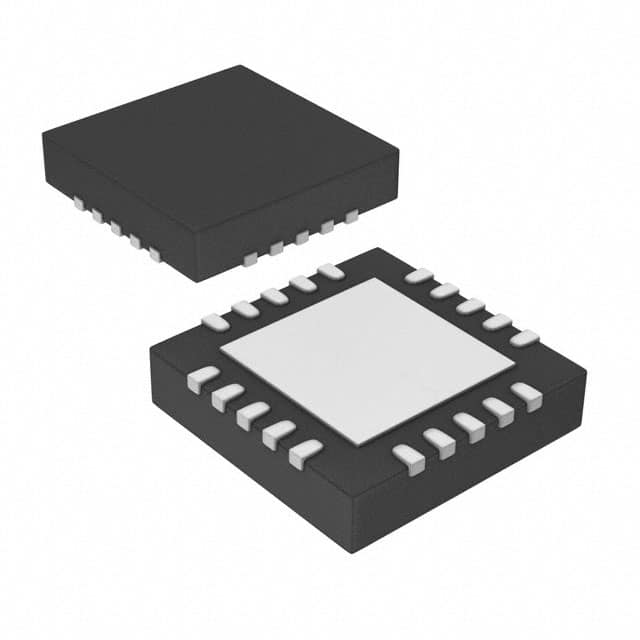
- Part No.:
- UCS1003-3-BP
- Manufacturer:
- Microchip Technology
- Category:
- Power Management - Specialized
- Package:
- 20-VFQFN Exposed Pad
- Datasheet:
-
 UCS1003-3-BP.pdf
- Description:
- IC USB PORT POWER CTRLR 20QFN
- Quantity:
- Payment:

- Shipping:

Inventory:406
Please send an inquiry. Send us your inquiry, and we will respond immediately.
Product details
Overview
UCS1003-3-BP from Microchip Technology is a USB port power controller with integrated charger emulation and attach detection, delivering up to 3.0A continuous current (2.85A typical) with 55 mΩ on-resistance, dynamic thermal regulation, and BC1.2/YD/T-1591/Apple/Samsung/RIM-compatible charging profiles. It operates across 2.9V–5.5V source voltage and supports wake-on-attach via A_DET# pin for low-power system standby states.
For engineers reviewing the UCS1003-3-BP datasheet, UCS1003-3-BP pinout, UCS1003-3-BP application, or UCS1003-3-BP equivalent, this device is selected for USB-C host-side power delivery control in battery-powered embedded systems requiring precise current limiting, multi-standard charger handshaking, and ultra-low-power attach detection without SMBus interface overhead.
Technical Context
The UCS1003-3-BP implements a dual-mode port power switch with selectable overcurrent trip or constant-current limiting, soft turn-on, UVLO/OVLO protection, backdrive/back-voltage blocking, and latch-or-auto-recovery fault handling. Its USB 2.0 high-speed data switch (RON_HSW = 2 Ω, BW = 1100 MHz) enables transparent SDP/CDP data pass-through while maintaining <200 ps total jitter at 480 Mbps.
Unlike the UCS1003-1, it lacks SMBus/I2C and current monitoring but includes dedicated A_DET# open-drain pin for low-power attach detection (IDET_QUAL = 800 µA, tDET_QUAL = 100 ms) and supports nine preloaded charger emulation profiles-including USB-IF BC1.2 CDP/DCP, YD/T-1591, and proprietary Apple/Samsung signatures-with 12W charging capability.
Key Specifications
| Parameter | Value and Actual Design Meaning |
|---|---|
| Max Continuous Current | 3.0A (2.85A typical); enables full USB BC1.2 DCP-level charging of smartphones and tablets without external FETs. |
| Port Power Switch RON | 55 mΩ (typical); minimizes voltage drop and power loss at 3A, supporting VBUS ≥ 2.0V under load. |
| Source Voltage Range | 2.9V to 5.5V; compatible with single-cell Li-ion (3.0–4.2V), USB PD sink rails, and 5V wall adapters. |
| Attach Detection Threshold | 800 µA (typical); reliably detects USB peripheral insertion during system sleep with ultra-low IDD_DETECT = 185 µA. |
| Thermal Shutdown Threshold | 135°C; protects against sustained overload or poor PCB thermal design by disabling VBUS output until die cools by 35°C. |
| Operating Temperature | –40°C to +85°C; qualified for industrial and mobile computing environments including notebooks and docking stations. |
| Package | 20-pin QFN (4 mm × 4 mm); exposes thermal pad (EP) for efficient heat dissipation in compact layouts. |
Pinout & Package
UCS1003-3-BP is housed in a 4 mm × 4 mm, 20-pin QFN package with exposed thermal pad (EP). Pin functions are validated per Microchip DS20005346B, page 2 (UCS1003-3 variant diagram).
| Pin/Terminal | Circuit Role | Design Meaning |
|---|---|---|
| 1, 20 | GND | Power ground reference; must be connected to low-impedance PCB ground plane with thermal vias to EP. |
| 2 | DMOUT | USB D− output to downstream device; actively driven during charger emulation and data pass-through. |
| 3, 4 | VBUS1, VBUS2 | USB VBUS output pins; paralleled internally to deliver up to 3.0A with shared 55 mΩ RON. |
| 5 | DMIN | USB D− input from upstream host; routed through high-speed switch to DMOUT in SDP/CDP modes. |
| 6 | DPIN | USB D+ input from upstream host; routed through high-speed switch to DPOUT in SDP/CDP modes. |
| 7 | SEL | Charger profile selection control; sets emulation mode (e.g., BC1.2 DCP vs. Apple 2.4A) via resistor ladder. |
| 8 | ALERT# | Open-drain fault indicator; asserts low on overcurrent, thermal shutdown, or VBUS discharge error. |
| 9, 10 | VS1, VS2 | Power switch input rails; accept 2.9–5.5V source; support split-supply configuration with VDD for standby optimization. |
| 11 | VDD | Digital supply (4.5–5.5V); powers logic, charger emulator, and attach detector; decoupling required near pin. |
| 12 | SMCLK/S0 | Not connected (NC) in UCS1003-3; reserved for SMBus clock in UCS1003-1 only. |
| 13 | EM_EN | Charger emulator enable; active-high control to activate BC1.2/YD/T-1591/Apple signature generation on DP/DM. |
| 14 | A_DET# | Open-drain attach detection output; pulls low when >800 µA detected on VBUS, enabling wake-from-sleep. |
| 15 | DPOUT | USB D+ output to downstream device; driven during emulation and passed through during data mode. |
| 16 | M2 | Mode select input; configures current limit level (ILIM2–ILIM8) via external resistor network per Table 1-2. |
| 17 | M1 | Mode select input; used with M2 to select among eight discrete current limit thresholds (570 mA to 3.0 A). |
| 18 | PWR_EN | Active-high power switch enable; controls VBUS1/VBUS2 output; supports latch or auto-recovery fault behavior. |
| 19 | SMDATA/LATCH | Not connected (NC) in UCS1003-3; reserved for SMBus data in UCS1003-1; LATCH function not implemented. |
| EP | Exposed Pad | Thermal and electrical ground; must be soldered to PCB ground plane with ≥9 thermal vias (0.3 mm diameter, 3×3 array). |
Key Features
| Feature | Design Value |
|---|---|
| Wake-on-Attach Detection | Ultra-low-power (185 µA) A_DET# pin triggers system wake from sleep/standby upon USB device insertion. |
| Nine Preloaded Charger Profiles | Hardware-based emulation of USB-IF BC1.2 CDP/DCP, YD/T-1591, Apple 2.4A, Samsung AFC, and RIM standards-no firmware required. |
| Dynamic Thermal Management | Reduces current limit at 110°C (TREG) with 10°C hysteresis; shuts down at 135°C (TTSD) with 35°C recovery margin. |
| Backdrive & Back-Voltage Protection | Prevents reverse current flow from VBUS into VS/VDD; blocks >150 mV back-voltage to avoid damage during hot-plug or adapter removal. |
| Soft Turn-On Rate Control | Controls dI/dt at 100 mA/µs to suppress inrush current and reduce EMI during VBUS ramp-up. |
Applications
| Notebook USB Charging Hub | Industrial Docking Station |
|---|---|
|
Use Scenario: Notebook with dual USB-A ports delivers fast charging to peripherals while maintaining USB 2.0 data integrity. IC Role / Device Role / Timing Role: UCS1003-3-BP acts as intelligent port power switch and BC1.2 charger emulator, managing VBUS delivery and DP/DM signature generation. Use Value: Enables 3.0A charging without host CPU intervention; A_DET# wake signal reduces system power consumption during idle. |
Use Scenario: Industrial docking station provides USB power and data to multiple field devices in factory automation. IC Role / Device Role / Timing Role: UCS1003-3-BP serves as robust port controller with thermal shutdown and latch-fault handling for unattended operation. Use Value: 55 mΩ RON ensures stable VBUS under 3A load; –40°C to +85°C rating supports wide ambient deployment. |
| AC-DC Wall Adapter w/ USB Port | Tablet Host-Side Power Manager |
|
Use Scenario: Compact wall adapter integrates USB-A port with smart charging for consumer electronics. IC Role / Device Role / Timing Role: UCS1003-3-BP replaces discrete FET + MCU solution, providing hardware-emulated charger signatures and OCL protection. Use Value: Eliminates firmware development; nine preloaded profiles ensure compatibility with legacy and modern smartphones. |
Use Scenario: Tablet motherboard manages USB OTG power delivery and peripheral attach detection during battery-powered operation. IC Role / Device Role / Timing Role: UCS1003-3-BP functions as low-quiescent-power USB port controller with wake-on-insert capability. Use Value: 5 µA sleep current and 185 µA detect current extend battery life; A_DET# enables instant wake without polling. |
Equivalent & Alternatives
The following parts are listed as comparable options for similar USB port power control applications.
| Alternative Part | Technical Difference | Application Difference | Selection Advice |
|---|---|---|---|
| TUSB211IRWBR | No charger emulation; USB 2.0 redriver only; no power switching or current limiting. | Used solely for signal integrity boost-not for power delivery or BC1.2 compliance. | Select only if USB data signal restoration is needed without power control. |
| TPS2546RTER | Integrated USB 2.0 switch + BC1.2 DCP/CDP emulator; supports 2.5A max; no A_DET# or wake-on-attach. | Lacks ultra-low-power attach detection; requires external microcontroller for wake management. | Choose when higher integration (integrated 5V LDO) is prioritized over sleep-state wake capability. |
Compared with TUSB211IRWBR and TPS2546RTER, UCS1003-3-BP uniquely combines 3.0A power switching, nine-hardware charger profiles, and A_DET#-based wake-on-attach in a single 4×4 mm QFN-enabling self-contained, firmware-free USB power control in battery-sensitive designs.
Availability
UCS1003-3-BP is available at Aetrix Electronics and suitable for notebook computers, industrial docking stations, and AC-DC wall adapters requiring stable component supply, long-term lifecycle support, and qualification for extended temperature operation.
Supply support for UCS1003-3-BP includes scheduled delivery planning, volume procurement assistance, BOM continuity management, traceable sourcing, and lifecycle availability coordination for OEM customers, industrial embedded developers, connected-device designers, and electronics production programs.
Manufacturer
Microchip Technology Inc. is a leading provider of microcontrollers, analog components, and USB interface solutions, with global manufacturing and quality certifications including ISO 9001 and AEC-Q200.
The UCS1003 family was designed specifically for USB host-side power delivery control in portable and embedded systems-emphasizing hardware-based charger emulation, thermal resilience, and ultra-low-power attach detection without software dependency.
FAQ
What is the primary function of the UCS1003-3-BP in a USB system?
The UCS1003-3-BP serves as a fully integrated USB port power controller that combines a 3.0A current-limited power switch, nine preloaded hardware-based charger emulation profiles (including BC1.2, YD/T-1591, Apple, and Samsung), and ultra-low-power attach detection via the A_DET# pin. Unlike the UCS1003-1, it omits SMBus interface and current monitoring, making it ideal for cost- and space-constrained host-side applications where firmware-free, reliable charging and wake-on-insert are critical. The UCS1003-3-BP does not require host processor involvement to initiate charging or detect attachment.
How does the UCS1003-3-BP differ from the UCS1003-1 and UCS1003-2 variants?
The UCS1003-3-BP is distinguished by its inclusion of the A_DET# open-drain attach detection pin and exclusion of SMBus/I2C interface and current monitoring circuitry-features present in the UCS1003-1. It shares the same nine preloaded charger profiles and current-limit selection (via M1/M2 resistors) with the UCS1003-2, but differs by using A_DET# instead of the CHRG# pin found on the UCS1003-2. This makes the UCS1003-3-BP optimal for systems requiring wake-from-sleep on USB insertion without SMBus overhead, whereas the UCS1003-1 suits applications needing programmable profiles and real-time current telemetry.
What current limit options are available on the UCS1003-3-BP, and how are they configured?
The UCS1003-3-BP supports eight discrete current limit settings-from 570 mA to 3.0 A-selected using external resistors on the M1 and M2 pins per Table 1-2 of DS20005346B. For example, M1 = 100 kΩ and M2 = 82 kΩ yields ILIM8 = 3.0 A (2.85A typical). These settings configure the port power switch's overcurrent threshold and constant-current limiting behavior. No software or register writes are needed; configuration is purely hardware-based via resistor ladders, ensuring deterministic behavior across power cycles and temperature ranges. The UCS1003-3-BP does not support dynamic reconfiguration after boot.
Does the UCS1003-3-BP support USB 2.0 high-speed data pass-through, and what are its signal integrity specs?
Yes, the UCS1003-3-BP integrates a USB 2.0-compliant high-speed data switch with 1100 MHz –3 dB bandwidth, <200 ps total jitter at 480 Mbps, and <25 ps propagation skew between DP and DM paths. Its on-resistance is 2 Ω (typical) at 5V, and off-isolation exceeds –30 dB at 240 MHz. The switch operates transparently in SDP and CDP modes, preserving eye diagram integrity as verified in Figures 2-1 and 2-2 of DS20005346B. It does not support USB 3.x or SuperSpeed; its data path is strictly USB 2.0 high-speed (480 Mbps) only.
What thermal protection mechanisms does the UCS1003-3-BP implement, and how do they affect operation?
The UCS1003-3-BP features three-tiered thermal protection: (1) Dynamic thermal regulation begins at 110°C (TREG), reducing current limit with 10°C hysteresis; (2) Thermal shutdown activates at 135°C (TTSD), turning off VBUS until die temperature drops by 35°C; and (3) Short-circuit response limits current within 1.5 µs and disconnects VBUS within 6 ms. These mechanisms prevent permanent damage during sustained overload or poor heatsinking. All thresholds are silicon-characterized-not trimmed-and operate independently of host control, ensuring fail-safe behavior even in unattended systems. The UCS1003-3-BP relies on PCB thermal vias to EP for effective heat transfer.
UCS1003-3-BP Specifications
- Product attributes
- Attribute value
- Manufacturer:
- Microchip Technology
- Series:
- -
- Package/Case:
- 20-VFQFN Exposed Pad
- Packaging:
- Tray
- Product Status:
- Active
- Applications:
- USB Dedicated Charging Port (DCP), Power Switch
- Current - Supply:
- 650µA
- Voltage - Supply:
- 4.5V ~ 5.5V
- Operating Temperature:
- -40°C ~ 125°C
- Grade:
- -
- Qualification:
- -
- Mounting Type:
- Surface Mount
- Supplier Device Package:
- 20-QFN (4x4)
UCS1003-3-BP FAQ
1.How can I place an order for UCS1003-3-BP through Aetrix?
Please submit a Request for Quotation (RFQ) for UCS1003-3-BP on Aetrix. Our sales agent will provide a competitive quotation and guide you through the order confirmation once you accept the terms.
2.Are the price and stock information for UCS1003-3-BP reliable?
The price and inventory of UCS1003-3-BP are updated periodically and may fluctuate due to market conditions. Stock and pricing data are typically refreshed every 24 hours. Quotation validity for UCS1003-3-BP is usually 5 days.
3.What payment methods are accepted for UCS1003-3-BP?
We accept Wire Transfer, PayPal, Credit Card, Western Union, MoneyGram, and Escrow for UCS1003-3-BP transactions.
Note: Certain payment methods may incur a processing fee.
4.How is shipping managed for UCS1003-3-BP?
UCS1003-3-BP orders can be shipped via leading logistics carriers, including DHL, UPS, FedEx, TNT, or Registered Mail.
Once your UCS1003-3-BP order is processed, you will receive an email with the shipment details and tracking number.
Note: Tracking information may take up to 24 hours to appear. Express delivery typically takes 3–5 business days.
5.How can I obtain technical support or documentation for UCS1003-3-BP?
For technical support, including UCS1003-3-BP datasheets, pinout diagrams, or application guidance, please contact our engineering support team. They can provide detailed documentation and assistance for your UCS1003-3-BP requirements.
6.How does Aetrix verify that UCS1003-3-BP is sourced from the original manufacturer or authorized distributors?
All UCS1003-3-BP products on Aetrix are procured from qualified distributors and authorized channels. Our dedicated quality assurance team conducts strict verification, including traceability checks and, if necessary, third-party testing. This ensures that UCS1003-3-BP meets industry standards.
7.What is the process for return or replacement of UCS1003-3-BP?
All UCS1003-3-BP units undergo pre-shipment inspection (PSI). If there is an issue with UCS1003-3-BP, returns or replacements are accepted under the following conditions:
1.Quantity discrepancies, incorrect items, or visible external defects (such as breakage or corrosion), acknowledged by Aetrix.
2.The issue is reported within 90 days of delivery.
3.The UCS1003-3-BP part is unused and in its original packaging.
Return procedure for UCS1003-3-BP:
1.Submit a request within 90 days.
2.Obtain a Return Material Authorization (RMA) from Aetrix.
UCS1003-3-BP Tags

-
TPS2511DGNR
Texas Instruments

-
UTC2000/MG
Microchip Technology

-
TUSB320HAIRWBR
Texas Instruments

-
TPS61252DSGR
Texas Instruments

-
PI5USB30216CXUAEX
Diodes Incorporated

-
SN6501DBVR
Texas Instruments

-
CYPD3177-24LQXQT
Infineon Technologies
-
SN6501QDBVRQ1
Texas Instruments

-
STUSB1600AQTR
STMicroelectronics

-
SN6505BDBVR
Texas Instruments
-
SN6501DBVT
Texas Instruments

-
TPS65150PWPR
Texas Instruments
Tech Hub

TTL and CMOS logic families differ in thresholds, loading, output drive, power and timing. This engineering guide compares 74HC and 74HCT, calculates noise margins and checks 3.3 V/5 V compatibility.

A practical engineering guide to 3.3V and 5V logic compatibility, input thresholds, resistor dividers, translator ICs, MOSFET level shifting, I2C pull-ups, timing limits and power-sequencing risks.

The 74HC595 uses push-pull logic outputs, while the TPIC6B595 uses 50 V open-drain DMOS sinks for higher-power loads. This guide compares timing, current limits, 3.3 V interfacing, load wiring, thermal…

The 74HC595 converts serial data into eight stable parallel outputs. This guide covers pin functions, shift and storage timing, OE and MR behavior, drive-current limits, cascading, voltage compatibilit…

A technical comparison of level-sensitive latches and edge-triggered flip-flops, covering timing windows, setup and hold limits, master–slave operation, time borrowing, race-through, HDL inference and…

A D latch stores one bit while Enable controls when data can pass. This reference covers gate-level operation, truth tables, transparency, setup and hold timing, LE versus OE, common ICs and practical …

An SR latch stores one bit through cross-coupled feedback. This engineering reference covers NOR and NAND implementations, truth tables, forbidden-state recovery, gated operation, switch debouncing, fa…

Latch circuits retain one bit through feedback. This technical reference covers SR and D latches, truth tables, transparency, timing limits, latch-versus-flip-flop behavior, applications and common log…

An engineering guide to LED driver operation, constant-current and constant-voltage outputs, linear and switching topologies, dimming, IC selection, calculations, replacement compatibility, and fault c…

Operational amplifier guide covering op amp basics, feedback, ideal vs real op amps, common configurations, buffer circuits, offset, bias current, gain-bandwidth, slew rate, rail-to-rail limits and sel…


