Send an Inquiry

To receive a quote for your project, please fill in the following information, and we’ll get back to you promptly.

Name*
Company*
Email Address*
Phone/WhatsApp
Part Number*
Quantity*
Message
Submit Inventory List

Please fill in the following information, and we’ll get back to you promptly.

Name*
Company*
Email Address*
Phone/WhatsApp
Upload My List
Message

Vishay General Semiconductor - Diodes Division VBUS54GD-FBL-G3-08
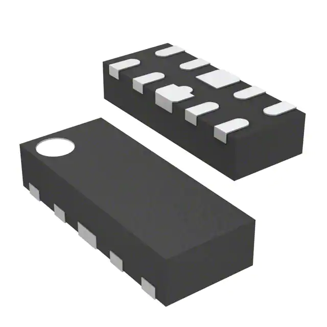
Part No.:
VBUS54GD-FBL-G3-08
Manufacturer:
Vishay General Semiconductor - Diodes Division
Category:
TVS Diodes
Package:
10-UFDFN
Datasheet:
AetrixVBUS54GD-FBL-G3-08.pdf
Description:
TVS DIODE 5.5VWM 15V LLP2510-10L
Quantity:
Payment:
Payment
Shipping:
Shipping

Inventory:3,982

Please send an inquiry. Send us your inquiry, and we will respond immediately.

Part Number
Quantity*
Price
Name*
Company
Email*
Comments

Product details

Overview

VBUS54GD-FBL-G3-08 from Vishay Semiconductors is a 4-line bidirectional ESD protection diode array in LLP2510-10M package, designed for high-speed data interfaces including USB 3.0, HDMI, DisplayPort, and Thunderbolt. It provides ±15 kV IEC 61000-4-2 contact/air discharge immunity, 0.3 pF inter-line capacitance, and clamps transients to ≤15 V at 3 A peak pulse current while operating up to 5.5 V DC.

For engineers reviewing the VBUS54GD-FBL-G3-08 datasheet, VBUS54GD-FBL-G3-08 pinout, VBUS54GD-FBL-G3-08 application, or VBUS54GD-FBL-G3-08 equivalent, this device delivers low-capacitance, flow-through layout compatibility, asymmetric bidirectional clamping, and MSL Level 1 solderability - critical for maintaining signal integrity on 480 Mbps to 1.65 Gbps differential data lines.

Technical Context

The VBUS54GD-FBL-G3-08 implements a Zener-based asymmetric bidirectional (BiAs) clamping architecture with matched D1+/D1− and D2+/D2− channel pairs. Its internal structure connects pins 3 and 8 to GND, uses pins 1/2/4/5 as active I/O terminals, and leaves pins 6/7/9/10 unconnected - enabling direct in-line placement without vias or trace discontinuities.

It achieves 0.6–0.75 pF line-to-ground capacitance at 1 MHz and 0 V bias, with only 0.3–0.4 pF between I/O lines, minimizing crosstalk and insertion loss. Clamping occurs at 9.1 V (typ.) for 1 A pulses and rises to 12–15 V at 3 A, while dynamic resistance remains ≤0.76 Ω under TLP stress.

Key Specifications

Parameter Value and Actual Design Meaning
ESD Immunity ±15 kV contact & air discharge per IEC 61000-4-2 - ensures robust handling in manufacturing and end-user environments
Clamping Voltage (IPPM = 3 A) 12–15 V - limits transient overvoltage to safe levels for 5.5 V-rated interface ICs
Inter-Line Capacitance 0.3–0.4 pF at 3.3 V - preserves signal rise/fall times and eye diagram integrity on USB 3.0/HDMI links
Reverse Standoff Voltage 5.5 V - matches standard USB/HDMI supply rails without leakage-induced logic errors
Leakage Current ≤0.1 μA at 5.5 V - prevents DC loading of high-impedance receiver inputs
Package LLP2510-10M (2.5 × 1.0 × 0.55 mm, 0.6 mm max height) - enables ultra-thin PCB designs and automated optical inspection
Peak Pulse Power 45 W per line (IEC 61000-4-5, 8/20 μs) - withstands surge events from cable coupling or board-level transients

Pinout & Package

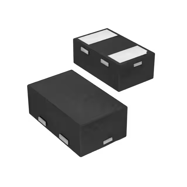
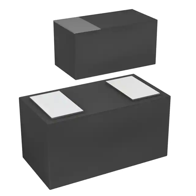
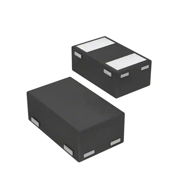
VBUS54GD-FBL-G3-08 uses the LLP2510-10M leadless plastic package (2.5 mm × 1.0 mm × 0.55 mm max), featuring a flow-through design optimized for high-speed differential traces. Pin 1 is marked by a dot; pins 3 and 8 are internally shorted GND terminals; pins 1/2 and 4/5 serve as matched D1+/D1− and D2+/D2− I/O pairs; pins 6/7/9/10 are NC.

Pin/Terminal Circuit Role Design Meaning
1, 2, 4, 5 Differential I/O (D1+, D1−, D2+, D2−) Active ESD protection paths - placed inline with data lanes to minimize impedance discontinuity
3, 8 GND Internally shorted ground reference - must be connected to system ground plane with low-inductance path
6, 7, 9, 10 No Connect (NC) Unbonded die pads - no PCB routing or thermal relief required

Key Features

Feature Design Value
Flow-through layout Enables straight PCB trace routing across pins 1–2 and 4–5 - eliminates stubs, vias, or bends that degrade 1.65 Gbps HDMI signals
Asymmetric bidirectional clamping Clamps negative transients below GND and positive transients above 5.5 V - protects both sides of differential receivers without biasing issues
0.3 pF inter-line capacitance Maintains <1% signal attenuation at 3 GHz - verified for HDMI 1.4 and USB 3.0 compliance
MSL Level 1 rating Supports reflow up to 260 °C/10 s without preconditioning - simplifies SMT assembly and eliminates moisture bake steps
e3 matte tin termination RoHS-compliant Sn plating with >1000-hr sulfur resistance - ensures long-term solder joint reliability in humid industrial enclosures

Applications

HDMI 1.4 Interface Protection USB 3.0 SuperSpeed Data Lines

Use Scenario: Protecting TMDS clock and data channels on HDMI source/sink PCBs against ESD during hot-plug and field operation.

IC Role / Device Role / Timing Role: In-line transient voltage suppressor on D0+/D0−, D1+/D1−, D2+/D2−, and CLK+/CLK− differential pairs.

Use Value: 0.3 pF inter-line capacitance prevents eye diagram closure; ±15 kV ESD rating meets IEC 61000-4-2 compliance for CE-marked consumer electronics.

Use Scenario: Safeguarding SSTX+/SSTX− and SSRX+/SSRX− lanes in USB 3.0 host/device controllers against connector-induced ESD.

IC Role / Device Role / Timing Role: Bidirectional clamping diode array placed immediately adjacent to USB Type-A/B/Type-C receptacles.

Use Value: 0.65 pF line-to-ground capacitance minimizes jitter accumulation; flow-through footprint avoids 5-GHz signal reflections.

DisplayPort 1.2 Differential Links Thunderbolt 1/2 Data Ports

Use Scenario: ESD hardening of DP0+/DP0− through DP3+/DP3− and AUX+/AUX− channels in monitors, docks, and GPUs.

IC Role / Device Role / Timing Role: Per-lane protection element with matched pair routing to preserve skew tolerance in 5.4 Gbps DP links.

Use Value: Matched D1+/D1− and D2+/D2− channel characteristics ensure <0.1 ps skew impact; 45 W pulse power handles cable discharge events.

Use Scenario: Transient suppression on Thunderbolt's dual-channel PCIe + DisplayPort multiplexed lanes in laptops and expansion chassis.

IC Role / Device Role / Timing Role: Dual-array implementation (e.g., 3× VBUS54GD-FBL-G3-08) covering Cio0/Cio1 TX/RX and Lsx control lines.

Use Value: Asymmetric clamping prevents false triggering on DC-coupled Thunderbolt PHYs; 0.55 mm profile fits tight space behind port connectors.

Equivalent & Alternatives

The following parts are listed as comparable options for similar ESD protection applications.

Alternative Part Technical Difference Application Difference Selection Advice
TPD4E05U06DQAR 0.5 pF inter-line capacitance; ±12 kV ESD rating; 1.6 mm × 1.6 mm X2SON package Higher capacitance limits use to USB 2.0 or lower-speed HDMI; larger footprint consumes more board area Select when cost sensitivity outweighs 0.2 pF capacitance advantage and board space permits larger package
ESD5451N 0.35 pF inter-line capacitance; ±15 kV ESD; 2.0 mm × 1.25 mm XSON-10 package; 6.5 V VRWM Slightly higher stand-off voltage suits 6 V auxiliary rails; different pinout requires layout revision Choose for mixed-voltage systems needing 6.5 V tolerance, but verify GND pin mapping and thermal pad compatibility

Compared with TPD4E05U06DQAR and ESD5451N, VBUS54GD-FBL-G3-08 offers the lowest inter-line capacitance (0.3 pF) and smallest footprint (2.5 × 1.0 mm) among 4-line ESD arrays, making it optimal for space-constrained, multi-gigabit interfaces where signal fidelity is non-negotiable.

Availability

VBUS54GD-FBL-G3-08 is available at Aetrix Electronics and suitable for HDMI 1.4, USB 3.0, and DisplayPort 1.2 applications requiring stable component supply, consistent parametric performance across production lots, and long-term lifecycle support.

Supply support for VBUS54GD-FBL-G3-08 includes scheduled delivery planning, volume procurement assistance, BOM continuity management, traceable sourcing, and lifecycle availability coordination for OEM customers, industrial embedded developers, connected-device designers, and electronics production programs.

Manufacturer

Vishay Intertechnology is a global semiconductor manufacturer specializing in discrete components, passive elements, and sensors, with leadership in precision resistors, power MOSFETs, and ESD protection devices.

The VBUS54GD-FBL-G3-08 belongs to Vishay's high-speed bus-port ESD protection product line, engineered specifically for preserving signal integrity on differential data interfaces operating beyond 1 Gbps while meeting stringent IEC 61000-4-2 immunity requirements.

FAQ

What is the maximum working voltage supported by VBUS54GD-FBL-G3-08?

The VBUS54GD-FBL-G3-08 has a reverse stand-off voltage (VRWM) of 5.5 V, meaning it reliably blocks voltages up to this level in normal operation without significant leakage. This matches standard USB 3.0 and HDMI supply rails. The device begins clamping at ~6.9 V breakdown and maintains safe operation up to its 125 °C junction temperature limit. VBUS54GD-FBL-G3-08 is not rated for continuous operation above 5.5 V DC.

Can VBUS54GD-FBL-G3-08 be used for single-ended signal lines like UART or I²C?

VBUS54GD-FBL-G3-08 is optimized for differential high-speed data lines (D1+/D1−, D2+/D2−) and relies on matched pair symmetry for minimal skew and crosstalk. Its 0.3 pF inter-line capacitance and asymmetric clamping are tailored for differential signaling. For single-ended interfaces such as UART or I²C, Vishay recommends dedicated single-line protectors like VBUS052CD-FAH, as VBUS54GD-FBL-G3-08's pinout and channel pairing do not align with typical single-ended routing.

Does VBUS54GD-FBL-G3-08 require external biasing or series resistors?

No, VBUS54GD-FBL-G3-08 operates passively with no external biasing or series components required. Its Zener-based clamping structure functions automatically during ESD events. The device is designed for direct in-line placement between connector and PHY, with pins 3 and 8 tied directly to a low-inductance ground plane. Series resistors would degrade signal integrity and are neither specified nor recommended in the official application schematics for USB 3.0 or HDMI.

How does the flow-through design of VBUS54GD-FBL-G3-08 improve signal integrity?

The flow-through design routes high-speed differential traces straight through pins 1→2 and 4→5 without vias, stubs, or layer transitions - preserving controlled impedance and minimizing reflections. Measured insertion loss remains <0.3 dB up to 3 GHz, and return loss exceeds 15 dB across the USB 3.0 and HDMI 1.4 bandwidth. This architecture directly addresses the 50 Ω surge impedance requirement of modern serial links, which VBUS54GD-FBL-G3-08 supports without compromising layout simplicity.

Is VBUS54GD-FBL-G3-08 compatible with lead-free reflow profiles?

Yes, VBUS54GD-FBL-G3-08 features e3 matte tin terminations and is qualified for lead-free reflow per J-STD-020. It supports peak temperatures up to 260 °C for 10 seconds at the terminals and carries MSL Level 1 rating - meaning it can be stored indefinitely at ambient conditions without baking. The LLP2510-10M package's low mass and uniform thermal response ensure reliable joint formation across all 10 terminals during standard Pb-free reflow cycles.

VBUS54GD-FBL-G3-08 Specifications

Product attributes
Attribute value
Manufacturer:
Vishay General Semiconductor - Diodes Division
Package/Case:
10-UFDFN
Series:
-
Packaging:
Tape & Reel (TR)
Product Status:
Obsolete
Type:
Steering (Rail to Rail)
Unidirectional Channels:
4
Bidirectional Channels:
-
Voltage - Reverse Standoff (Typ):
5.5V (Max)
Voltage - Breakdown (Min):
6.9V
Voltage - Clamping (Max) @ Ipp:
15V
Current - Peak Pulse (10/1000µs):
3A (8/20µs)
Power - Peak Pulse:
45W
Power Line Protection:
Yes
Applications:
HDMI
Capacitance @ Frequency:
-
Operating Temperature:
-40°C ~ 125°C (TJ)
Grade:
-
Qualification:
-
Mounting Type:
Surface Mount
Supplier Device Package:
LLP2510-10L

VBUS54GD-FBL-G3-08 FAQ

1.How can I place an order for VBUS54GD-FBL-G3-08 through Aetrix?

Please submit a Request for Quotation (RFQ) for VBUS54GD-FBL-G3-08 on Aetrix. Our sales agent will provide a competitive quotation and guide you through the order confirmation once you accept the terms.

2.Are the price and stock information for VBUS54GD-FBL-G3-08 reliable?

The price and inventory of VBUS54GD-FBL-G3-08 are updated periodically and may fluctuate due to market conditions. Stock and pricing data are typically refreshed every 24 hours. Quotation validity for VBUS54GD-FBL-G3-08 is usually 5 days.

3.What payment methods are accepted for VBUS54GD-FBL-G3-08?

We accept Wire Transfer, PayPal, Credit Card, Western Union, MoneyGram, and Escrow for VBUS54GD-FBL-G3-08 transactions.

Note: Certain payment methods may incur a processing fee.

4.How is shipping managed for VBUS54GD-FBL-G3-08?

VBUS54GD-FBL-G3-08 orders can be shipped via leading logistics carriers, including DHL, UPS, FedEx, TNT, or Registered Mail.

Once your VBUS54GD-FBL-G3-08 order is processed, you will receive an email with the shipment details and tracking number.

Note: Tracking information may take up to 24 hours to appear. Express delivery typically takes 3–5 business days.

5.How can I obtain technical support or documentation for VBUS54GD-FBL-G3-08?

For technical support, including VBUS54GD-FBL-G3-08 datasheets, pinout diagrams, or application guidance, please contact our engineering support team. They can provide detailed documentation and assistance for your VBUS54GD-FBL-G3-08 requirements.

6.How does Aetrix verify that VBUS54GD-FBL-G3-08 is sourced from the original manufacturer or authorized distributors?

All VBUS54GD-FBL-G3-08 products on Aetrix are procured from qualified distributors and authorized channels. Our dedicated quality assurance team conducts strict verification, including traceability checks and, if necessary, third-party testing. This ensures that VBUS54GD-FBL-G3-08 meets industry standards.

7.What is the process for return or replacement of VBUS54GD-FBL-G3-08?

All VBUS54GD-FBL-G3-08 units undergo pre-shipment inspection (PSI). If there is an issue with VBUS54GD-FBL-G3-08, returns or replacements are accepted under the following conditions:

1.Quantity discrepancies, incorrect items, or visible external defects (such as breakage or corrosion), acknowledged by Aetrix.

2.The issue is reported within 90 days of delivery.

3.The VBUS54GD-FBL-G3-08 part is unused and in its original packaging.

Return procedure for VBUS54GD-FBL-G3-08:

1.Submit a request within 90 days.

2.Obtain a Return Material Authorization (RMA) from Aetrix.

VBUS54GD-FBL-G3-08 Tags
  • VBUS54GD-FBL-G3-08
  • VBUS54GD-FBL-G3-08 PDF
  • VBUS54GD-FBL-G3-08 Datasheet
  • VBUS54GD-FBL-G3-08 Specifications
  • VBUS54GD-FBL-G3-08 Images
  • Vishay General Semiconductor - Diodes Division
  • Vishay General Semiconductor - Diodes Division VBUS54GD-FBL-G3-08
  • Buy VBUS54GD-FBL-G3-08
  • VBUS54GD-FBL-G3-08 Price
  • VBUS54GD-FBL-G3-08 Distributor
  • VBUS54GD-FBL-G3-08 Supplier
  • VBUS54GD-FBL-G3-08 Wholesale
Related Products
ESD9B5.0ST5G
ESD9B5.0ST5G

onsemi

DESD3V3E1BL-7B
DESD3V3E1BL-7B

Diodes Incorporated

ESD5Z3.3T1G
ESD5Z3.3T1G

onsemi

D5V0H1B2LP-7B
D5V0H1B2LP-7B

Diodes Incorporated

D5V0P1B2LP-7B
D5V0P1B2LP-7B

Diodes Incorporated

DESD5V0U1BA-7
DESD5V0U1BA-7

Diodes Incorporated

ESD5Z5.0T1G
ESD5Z5.0T1G

onsemi

DESD5V0U1BB-7
DESD5V0U1BB-7

Diodes Incorporated

D12V0L1B2LP-7B
D12V0L1B2LP-7B

Diodes Incorporated

PESD2V0Y1BSFYL
PESD2V0Y1BSFYL

Nexperia USA Inc.

DF2S5M4CT,L3F
DF2S5M4CT,L3F

Toshiba Semiconductor and Storage

D5V0L1B2WS-7
D5V0L1B2WS-7

Diodes Incorporated

Tech Hub
Search

Search

PRODUCT

PRODUCT

PHONE

PHONE

USER

USER