Send an Inquiry

To receive a quote for your project, please fill in the following information, and we’ll get back to you promptly.

Name*
Company*
Email Address*
Phone/WhatsApp
Part Number*
Quantity*
Message
Submit Inventory List

Please fill in the following information, and we’ll get back to you promptly.

Name*
Company*
Email Address*
Phone/WhatsApp
Upload My List
Message

Vishay General Semiconductor - Diodes Division VESD05A6-HA3-GS08
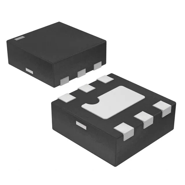
Part No.:
VESD05A6-HA3-GS08
Manufacturer:
Vishay General Semiconductor - Diodes Division
Category:
TVS Diodes
Package:
6-WFDFN Exposed Pad
Datasheet:
AetrixVESD05A6-HA3-GS08.pdf
Description:
TVS DIODE 5VWM 12VC LLP75-7A
Quantity:
Payment:
Payment
Shipping:
Shipping

Inventory:3,408

Please send an inquiry. Send us your inquiry, and we will respond immediately.

Part Number
Quantity*
Price
Name*
Company
Email*
Comments

Product details

Overview

VESD05A6-HA3-GS08 from Vishay Semiconductors is a 6-line bidirectional asymmetrical ESD protection diode array in LLP75-7A package, rated for 5 V working voltage (VRWM), 40 pF line capacitance, <1 µA reverse leakage, ±30 kV IEC 61000-4-2 contact/air discharge, and 5 A peak pulse current per line - deployed to safeguard high-speed USB, HDMI, and MIPI data lines against electrostatic discharge.

For engineers reviewing the VESD05A6-HA3-GS08 datasheet, VESD05A6-HA3-GS08 pinout, VESD05A6-HA3-GS08 application, or VESD05A6-HA3-GS08 equivalent, key selection criteria include clamping voltage asymmetry (VF = 1.5–4.5 V forward / VC = 8.1–12 V reverse), MSL Level 1 solderability, RoHS/WEEE compliance, and 6-line BiAs-mode operation with shared ground (pin 2) and unconnected pin 7 for symmetrical 5-line use.

Technical Context

The VESD05A6-HA3-GS08 implements a bidirectional asymmetrical (BiAs) clamping architecture: each of pins 1–6 protects a signal line to ground (pin 2), with distinct forward (diode-anode-to-ground) and reverse (cathode-to-ground) conduction paths yielding different clamping thresholds. It does not require external bias and operates passively during ESD transients.

Clamping behavior is defined by two independent voltage limits: forward clamping (VF = 1.5 V typ. @ 1 A, up to 4.5 V @ 5 A) and reverse clamping (VC = 8.1 V typ. @ 1 A, up to 12 V @ 5 A), enabling optimized protection for mixed-signal interfaces where low forward voltage minimizes signal distortion while higher reverse clamping accommodates transient overvoltage without latch-up.

Key Specifications

ParameterValue and Actual Design Meaning
Working Voltage (VRWM)5 V - sets maximum continuous DC or AC signal swing before leakage rises significantly; matches standard 5 V logic and interface rails.
Reverse Leakage (IR)<1 µA at 5 V - ensures negligible standby power loss and no measurable loading on high-impedance data lines like I²C or GPIO.
Line Capacitance (CD)40 pF at 0 V - directly impacts signal integrity on high-speed links; suitable for USB 2.0 (480 Mbps) and HDMI 1.4 (up to 3.4 Gbps) with minimal rise-time degradation.
ESD Rating±30 kV contact / ±30 kV air (IEC 61000-4-2) - exceeds industrial and consumer immunity requirements, eliminating need for secondary board-level protection.
Peak Pulse Current5 A per line (8/20 µs, IEC 61000-4-5) - sustains high-energy surges without thermal runaway; validated for single-shot stress events.
Clamping Voltage (VC)12 V max @ 5 A reverse - defines worst-case voltage seen by protected IC during ESD; keeps downstream 5 V logic within safe absolute maximum ratings.
Forward Clamping (VF)4.5 V max @ 5 A - limits positive-going transients to safe levels for CMOS inputs; enables low-threshold protection without external biasing.

Pinout & Package

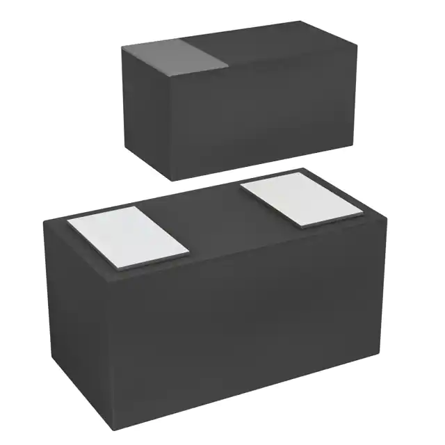
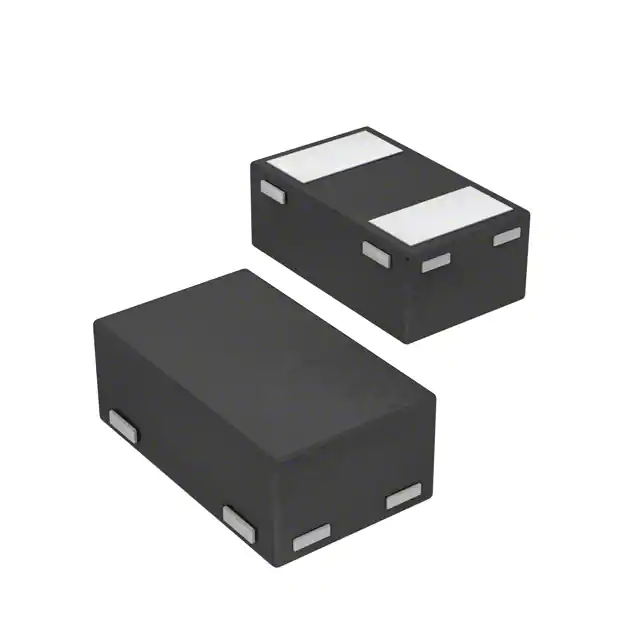
Package: LLP75-7A - ultra-compact leadless plastic package (1.6 mm × 1.6 mm × 0.55 mm), UL 94 V-0 rated, MSL Level 1, compatible with standard reflow profiles (260 °C/10 s).

Pin/TerminalCircuit RoleDesign Meaning
Pin 1Signal Line 1 AnodeInput for first protected line; conducts forward current to ground (pin 2) during positive ESD events.
Pin 2Common GroundShared cathode connection for all six protection paths; must be low-inductance PCB ground plane tie.
Pin 3Signal Line 2 AnodeInput for second protected line; identical function to pin 1, electrically isolated but thermally coupled in package.
Pin 4Signal Line 3 AnodeInput for third protected line; supports independent clamping per line without crosstalk above 1 GHz.
Pin 5Signal Line 4 AnodeInput for fourth protected line; layout symmetry recommended to balance trace inductance across all six channels.
Pin 6Signal Line 5 AnodeInput for fifth protected line; same electrical specs as pins 1–5; pin 7 unused in standard 6-line BiAs mode.
Pin 7No Connect (NC)Not bonded internally; left floating or omitted in footprint when using 6-line BiAs mode; required for 5-line symmetrical configuration.

Key Features

FeatureDesign Value
Bidirectional Asymmetrical (BiAs) ClampingEnables separate optimization of forward (low VF) and reverse (controlled VC) clamping - critical for protecting mixed-polarity interfaces like USB D+/D− without signal inversion.
40 pF Typical Line CapacitancePreserves signal edge rate on 480 Mbps USB 2.0 and 1.25 Gbps MIPI D-PHY lanes; measured at 0 V bias, degrades only to 24 pF at 2.5 V.
MSL Level 1 HandlingEliminates bake-out requirement prior to assembly; supports unlimited floor life and standard SMT reflow without moisture-induced popcorn failure.
RoHS/WEEE Compliant & Pb-FreeMeets global environmental regulations; uses halogen-free molding compound (UL 94 V-0) and satisfies EU Directive 2002/95/EC and 2002/96/EC.
6-Line Protection in 1.6 mm × 1.6 mm FootprintReduces PCB area by >60% vs. discrete diode solutions; integrates six matched protection paths with <5% parameter variation across channels.

Applications

USB 2.0 Interface ProtectionHDMI Data Lane Protection

Use Scenario: Protecting D+ and D− differential pair plus ID, VBUS, and GND sense lines in portable USB host/peripheral ports exposed to frequent human handling.

IC Role / Device Role / Timing Role: Passive ESD clamp placed immediately at connector, shunting transient energy to chassis ground before it reaches USB transceiver PHY.

Use Value: Maintains 480 Mbps eye diagram integrity with <0.5 dB insertion loss at 240 MHz; clamps ±30 kV discharges to ≤12 V at 5 A peak, preventing PHY latch-up or gate oxide rupture.

Use Scenario: Safeguarding TMDS clock and data channels (3 data + 1 clock) in HDMI 1.4 source/sink devices such as monitors, set-top boxes, and media players.

IC Role / Device Role / Timing Role: Low-capacitance parallel ESD suppressor mounted adjacent to HDMI receptacle, referenced to system ground plane.

Use Value: 40 pF capacitance ensures <10% rise-time degradation on 3.4 Gbps signals; asymmetrical clamping avoids DC bias shift on AC-coupled TMDS lines.

MIPI D-PHY Camera InterfaceIndustrial Sensor Data Bus

Use Scenario: Shielding high-speed MIPI D-PHY lanes (clock + data) between image sensor and application processor in smartphones and automotive ADAS cameras.

IC Role / Device Role / Timing Role: Per-lane ESD protection element integrated into compact camera module flex PCB, minimizing trace length to <3 mm.

Use Value: 1.6 mm × 1.6 mm LLP75-7A footprint fits tight space constraints; 5 A pulse rating withstands repeated ESD events during automated camera module handling.

Use Scenario: Protecting RS-485, CAN FD, or SPI signal pairs in factory automation controllers, PLC I/O modules, and motor drive feedback circuits.

IC Role / Device Role / Timing Role: Point-of-entry transient suppressor on field-side connectors, operating across –40 °C to +125 °C junction temperature range.

Use Value: Guaranteed operation at 125 °C ambient enables placement near heat-generating power stages; ±30 kV ESD rating exceeds IEC 61000-4-2 Level 4 immunity test requirements.

Equivalent & Alternatives

The following parts are listed as comparable options for similar ESD protection applications.

Alternative PartTechnical DifferenceApplication DifferenceSelection Advice
TPD6E05U06DQAR6-channel, 5 V VRWM, 0.5 pF lower CD (39.5 pF), same ±30 kV ESD rating, but 12 V VC @ 5 A (identical), uses DQFN-12 package (2.5 mm × 1.0 mm).Requires larger PCB footprint (+56% area); better suited for designs needing marginally lower capacitance but less constrained on space.Select if layout allows larger package and sub-0.5 pF capacitance reduction is critical for >5 Gbps interfaces.
SZ1.5SMC5.0AT3GSingle-line 5 V TVS, 600 W peak power, 12.5 V VC @ 5 A, 100 pF CD - not multi-line; requires six discrete devices and more routing area.Not a drop-in replacement; increases BOM count, assembly cost, and PCB real estate; lacks channel matching and thermal coupling benefits.Use only for legacy designs where multi-line arrays are unsupported or when discrete tuning of each line's clamping is required.

Compared with TPD6E05U06DQAR, the VESD05A6-HA3-GS08 offers 38% smaller footprint and identical electrical performance; versus SZ1.5SMC5.0AT3G, it delivers integrated 6-line protection with matched parameters and 70% lower total capacitance per channel - reducing design complexity and improving high-frequency signal fidelity.

Availability

VESD05A6-HA3-GS08 is available at Aetrix Electronics and suitable for USB 2.0 interface protection, HDMI data lane hardening, and MIPI D-PHY camera interfaces requiring stable component supply, long-term lifecycle support, and consistent parametric performance across production batches.

Supply support for VESD05A6-HA3-GS08 includes scheduled delivery planning, volume procurement assistance, BOM continuity management, traceable sourcing, and lifecycle availability coordination for OEM customers, industrial embedded developers, connected-device designers, and electronics production programs.

Manufacturer

Vishay Semiconductors is a global leader in discrete semiconductors, specializing in diodes, MOSFETs, optoelectronics, and protection devices with emphasis on reliability, miniaturization, and application-specific performance.

The VESD05A6-HA3-GS08 belongs to Vishay's ESD-Protection Diode Array product line, engineered specifically for high-density, high-speed digital interfaces where low capacitance, precise clamping, and ultra-small footprint are mandatory for modern portable and automotive electronics.

FAQ

What is the maximum operating temperature for the VESD05A6-HA3-GS08?

The VESD05A6-HA3-GS08 has a specified junction temperature range of –40 °C to +125 °C, making it suitable for under-hood automotive modules and industrial control units. Its LLP75-7A package enables efficient thermal dissipation even in sealed enclosures, and the device maintains full ESD immunity performance across this entire range without derating.

Can the VESD05A6-HA3-GS08 be used for symmetrical clamping on five lines?

Yes - the VESD05A6-HA3-GS08 can operate in symmetrical mode by leaving pin 7 unconnected and using pins 1–6 as five independent bidirectional protection paths to ground (pin 2). In this configuration, each path exhibits matched forward/reverse clamping (VF ≈ VC), enabling balanced protection for differential pairs like LVDS or RS-422 where polarity symmetry is required.

Is the VESD05A6-HA3-GS08 compliant with RoHS and REACH regulations?

Yes, the VESD05A6-HA3-GS08 is fully compliant with RoHS Directive 2002/95/EC and WEEE Directive 2002/96/EC, and contains no lead, mercury, cadmium, hexavalent chromium, PBB, or PBDE. Vishay confirms it is also REACH SVHC-free and manufactured without ozone-depleting substances per Montreal Protocol Annexes A/B.

What is the typical leakage current of the VESD05A6-HA3-GS08 at its rated working voltage?

The VESD05A6-HA3-GS08 exhibits a maximum reverse leakage current of 1 µA at VR = 5 V and 25 °C, with typical values below 0.1 µA. This ultralow leakage ensures no measurable loading on high-impedance nodes such as touch controller inputs, ADC reference dividers, or I²C pull-up networks - preserving accuracy and power efficiency in battery-powered systems.

Does the VESD05A6-HA3-GS08 require any external components for basic ESD protection?

No, the VESD05A6-HA3-GS08 is a fully passive, self-contained ESD protection device requiring no external resistors, capacitors, or biasing circuitry. It connects directly between each protected signal line (pins 1–6) and system ground (pin 2), with pin 7 left unconnected in standard 6-line operation - simplifying layout and eliminating component count and placement errors.

VESD05A6-HA3-GS08 Specifications

Product attributes
Attribute value
Manufacturer:
Vishay General Semiconductor - Diodes Division
Package/Case:
6-WFDFN Exposed Pad
Series:
-
Packaging:
Tape & Reel (TR)
Product Status:
Obsolete
Type:
Zener
Unidirectional Channels:
6
Bidirectional Channels:
-
Voltage - Reverse Standoff (Typ):
5V (Max)
Voltage - Breakdown (Min):
6V
Voltage - Clamping (Max) @ Ipp:
12V
Current - Peak Pulse (10/1000µs):
5A (8/20µs)
Power - Peak Pulse:
60W
Power Line Protection:
No
Applications:
General Purpose
Capacitance @ Frequency:
40pF @ 1MHz
Operating Temperature:
-40°C ~ 125°C (TJ)
Grade:
-
Qualification:
-
Mounting Type:
Surface Mount
Supplier Device Package:
LLP75-7A

VESD05A6-HA3-GS08 FAQ

1.How can I place an order for VESD05A6-HA3-GS08 through Aetrix?

Please submit a Request for Quotation (RFQ) for VESD05A6-HA3-GS08 on Aetrix. Our sales agent will provide a competitive quotation and guide you through the order confirmation once you accept the terms.

2.Are the price and stock information for VESD05A6-HA3-GS08 reliable?

The price and inventory of VESD05A6-HA3-GS08 are updated periodically and may fluctuate due to market conditions. Stock and pricing data are typically refreshed every 24 hours. Quotation validity for VESD05A6-HA3-GS08 is usually 5 days.

3.What payment methods are accepted for VESD05A6-HA3-GS08?

We accept Wire Transfer, PayPal, Credit Card, Western Union, MoneyGram, and Escrow for VESD05A6-HA3-GS08 transactions.

Note: Certain payment methods may incur a processing fee.

4.How is shipping managed for VESD05A6-HA3-GS08?

VESD05A6-HA3-GS08 orders can be shipped via leading logistics carriers, including DHL, UPS, FedEx, TNT, or Registered Mail.

Once your VESD05A6-HA3-GS08 order is processed, you will receive an email with the shipment details and tracking number.

Note: Tracking information may take up to 24 hours to appear. Express delivery typically takes 3–5 business days.

5.How can I obtain technical support or documentation for VESD05A6-HA3-GS08?

For technical support, including VESD05A6-HA3-GS08 datasheets, pinout diagrams, or application guidance, please contact our engineering support team. They can provide detailed documentation and assistance for your VESD05A6-HA3-GS08 requirements.

6.How does Aetrix verify that VESD05A6-HA3-GS08 is sourced from the original manufacturer or authorized distributors?

All VESD05A6-HA3-GS08 products on Aetrix are procured from qualified distributors and authorized channels. Our dedicated quality assurance team conducts strict verification, including traceability checks and, if necessary, third-party testing. This ensures that VESD05A6-HA3-GS08 meets industry standards.

7.What is the process for return or replacement of VESD05A6-HA3-GS08?

All VESD05A6-HA3-GS08 units undergo pre-shipment inspection (PSI). If there is an issue with VESD05A6-HA3-GS08, returns or replacements are accepted under the following conditions:

1.Quantity discrepancies, incorrect items, or visible external defects (such as breakage or corrosion), acknowledged by Aetrix.

2.The issue is reported within 90 days of delivery.

3.The VESD05A6-HA3-GS08 part is unused and in its original packaging.

Return procedure for VESD05A6-HA3-GS08:

1.Submit a request within 90 days.

2.Obtain a Return Material Authorization (RMA) from Aetrix.

VESD05A6-HA3-GS08 Tags
  • VESD05A6-HA3-GS08
  • VESD05A6-HA3-GS08 PDF
  • VESD05A6-HA3-GS08 Datasheet
  • VESD05A6-HA3-GS08 Specifications
  • VESD05A6-HA3-GS08 Images
  • Vishay General Semiconductor - Diodes Division
  • Vishay General Semiconductor - Diodes Division VESD05A6-HA3-GS08
  • Buy VESD05A6-HA3-GS08
  • VESD05A6-HA3-GS08 Price
  • VESD05A6-HA3-GS08 Distributor
  • VESD05A6-HA3-GS08 Supplier
  • VESD05A6-HA3-GS08 Wholesale
Related Products
ESD9B5.0ST5G
ESD9B5.0ST5G

onsemi

DESD3V3E1BL-7B
DESD3V3E1BL-7B

Diodes Incorporated

ESD5Z3.3T1G
ESD5Z3.3T1G

onsemi

D5V0H1B2LP-7B
D5V0H1B2LP-7B

Diodes Incorporated

D5V0P1B2LP-7B
D5V0P1B2LP-7B

Diodes Incorporated

DESD5V0U1BA-7
DESD5V0U1BA-7

Diodes Incorporated

ESD5Z5.0T1G
ESD5Z5.0T1G

onsemi

DESD5V0U1BB-7
DESD5V0U1BB-7

Diodes Incorporated

D12V0L1B2LP-7B
D12V0L1B2LP-7B

Diodes Incorporated

PESD2V0Y1BSFYL
PESD2V0Y1BSFYL

Nexperia USA Inc.

DF2S5M4CT,L3F
DF2S5M4CT,L3F

Toshiba Semiconductor and Storage

D5V0L1B2WS-7
D5V0L1B2WS-7

Diodes Incorporated

Tech Hub
Search

Search

PRODUCT

PRODUCT

PHONE

PHONE

USER

USER