Send an Inquiry

To receive a quote for your project, please fill in the following information, and we’ll get back to you promptly.

Name*
Company*
Email Address*
Phone/WhatsApp
Part Number*
Quantity*
Message
Submit Inventory List

Please fill in the following information, and we’ll get back to you promptly.

Name*
Company*
Email Address*
Phone/WhatsApp
Upload My List
Message

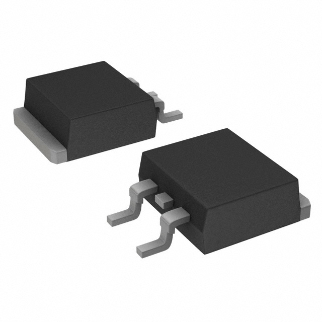
Vishay General Semiconductor - Diodes Division VS-6CWQ04FNTRRPBF
Part No.:
VS-6CWQ04FNTRRPBF
Manufacturer:
Vishay General Semiconductor - Diodes Division
Category:
Diode Arrays
Package:
TO-252-3, DPAK (2 Leads + Tab), SC-63
Datasheet:
AetrixVS-6CWQ04FNTRRPBF.pdf
Description:
DIODE ARRAY SCHOTT 40V 3.5A DPAK
Quantity:
Payment:
Payment
Shipping:
Shipping

Inventory:6,300

Please send an inquiry. Send us your inquiry, and we will respond immediately.

Part Number
Quantity*
Price
Name*
Company
Email*
Comments

Product details

Overview

VS-6CWQ04FNTRRPBF from Vishay Semiconductors is a high-performance dual common-cathode Schottky rectifier in D-PAK (TO-252AA) package, rated for 40 V reverse voltage and 3.5 A average forward current per leg (7 A total device), with 0.49 V forward voltage at 3 A and 125 °C - optimized for compact DC/DC converters and battery protection circuits.

For engineers reviewing the VS-6CWQ04FNTRRPBF datasheet, VS-6CWQ04FNTRRPBF pinout, VS-6CWQ04FNTRRPBF application, or VS-6CWQ04FNTRRPBF equivalent, key selection criteria include low VF at high junction temperature, center-tap common-cathode topology, MSL Level 1 surface-mount compatibility, and avalanche energy rating of 8 mJ per leg.

Technical Context

This dual-leg Schottky rectifier uses a monolithic center-tapped die structure with guard ring passivation to ensure ruggedness and long-term reliability under repetitive surge and thermal cycling. Its low forward slope resistance (37.33 mΩ) and low junction capacitance (189 pF at 5 V) support high-frequency switching up to MHz-range operation in synchronous rectification and freewheeling roles.

The device operates across -40 °C to +150 °C junction temperature range, with thermal resistance of 4.70 °C/W per leg (2.35 °C/W per device), enabling efficient heat transfer to PCB copper when mounted on a thermally enhanced pad. It meets J-STD-020 MSL Level 1 and is lead (Pb)-free compliant.

Key Specifications

Parameter Value and Actual Design Meaning
VR (Max DC Reverse Voltage) 40 V - supports input rails up to 36 V nominal in industrial and automotive power supplies.
IF(AV) per leg 3.5 A - enables continuous 7 A total output in dual-phase or parallel-leg configurations.
VF at 3 A, 125 °C 0.49 V - reduces conduction loss by ~30% vs. standard Schottky diodes at elevated temperature.
EAS per leg 8.0 mJ - withstands transient energy during inductive load switching without failure.
RthJC per leg 4.70 °C/W - allows direct thermal coupling to PCB ground plane for passive cooling in space-constrained designs.
CT at 5 V 189 pF - minimizes capacitive switching loss and EMI in >100 kHz SMPS topologies.
dV/dt rating 10,000 V/μs - prevents false turn-on in fast-switching half-bridge or LLC resonant circuits.

Pinout & Package

D-PAK (TO-252AA) surface-mount package with exposed thermal pad on underside; 3-pin configuration (two anodes + shared cathode tab); compatible with standard reflow profiles (peak 260 °C, MSL Level 1).

Pin/Terminal Circuit Role Design Meaning
Pin 1 (Anode A) First anode connection Accepts forward current from first switching leg; electrically isolated from Pin 3.
Pin 2 (Cathode) Common cathode terminal Shared return path for both legs; large metal tab provides primary thermal conduction path to PCB.
Pin 3 (Anode B) Second anode connection Accepts forward current from second switching leg; symmetrical layout enables balanced PCB routing.

Key Features

Feature Design Value
Center-tap common-cathode architecture Enables dual independent rectification paths sharing one thermal and electrical return node - simplifies layout in dual-output or center-tapped transformer designs.
Guard ring passivation Prevents edge breakdown under high dv/dt and high VR stress, extending lifetime in noisy industrial environments.
Low VF slope with temperature VF increases only marginally from 0.53 V (25 °C) to 0.49 V (125 °C) at 3 A - maintains efficiency over full operating range.
MSL Level 1 rating Allows unlimited floor life and single reflow without baking - reduces manufacturing overhead in high-volume SMT lines.
Lead (Pb)-free and RoHS-compliant Meets global environmental regulations without compromising thermal or electrical performance.

Applications

Server Power Supply USB-C PD Charger

Use Scenario: Secondary-side synchronous rectification in 48 V–12 V intermediate bus converter.

IC Role / Device Role / Timing Role: Dual-leg Schottky rectifier replacing MOSFETs in cost-sensitive designs where gate drive complexity must be avoided.

Use Value: Delivers 0.49 V VF at 125 °C to maintain >94% efficiency at full load while reducing component count versus discrete dual-diode solutions.

Use Scenario: Output rectification in 20 V/5 A USB-C power delivery adapter with dual-port capability.

IC Role / Device Role / Timing Role: Common-cathode dual anode rectifier supplying two independent 5 V/3 A outputs from a shared transformer winding.

Use Value: Enables compact layout with shared thermal pad and eliminates need for two separate diodes and associated trace area.

Battery Protection Circuit Automotive Infotainment DC/DC

Use Scenario: Reverse-polarity and backfeed protection in 12 V LiFePO₄ battery bank systems.

IC Role / Device Role / Timing Role: Low-VF freewheeling path preventing damage during hot-swap or accidental polarity reversal.

Use Value: 8 mJ avalanche energy rating absorbs inductive kickback from solenoid loads without clamping diode or TVS supplementation.

Use Scenario: Input rectification in 12 V–3.3 V buck converter powering infotainment head unit MCU and display drivers.

IC Role / Device Role / Timing Role: High-frequency Schottky rectifier handling 300 kHz switching with minimal EMI generation.

Use Value: 189 pF junction capacitance and 10,000 V/μs dV/dt rating prevent parasitic turn-on and reduce conducted emissions in automotive EMC testing.

Equivalent & Alternatives

The following parts are listed as comparable options for similar dual common-cathode Schottky rectifier applications.

Alternative Part Technical Difference Application Difference Selection Advice
STPS745D 45 V VR, 3.5 A per leg, VF = 0.55 V @ 3 A / 125 °C, TO-252 package, no specified EAS rating Lacks avalanche energy spec; higher VF increases conduction loss in thermally constrained designs Preferred where VR margin >5 V is required and thermal budget permits higher VF penalty
MBR1045CT 45 V VR, 5 A per leg, VF = 0.75 V @ 5 A / 25 °C, TO-220AC package, no MSL rating Through-hole, higher VF, no surface-mount compliance - unsuitable for automated SMT assembly Only viable for legacy through-hole designs or prototyping where reflow compatibility is not required

Compared with STPS745D and MBR1045CT, the VS-6CWQ04FNTRRPBF offers superior thermal performance (4.70 °C/W vs. ≥10 °C/W), lower VF at high temperature, MSL Level 1 compliance, and documented 8 mJ avalanche robustness - making it the preferred choice for high-density, high-reliability SMT power conversion.

Availability

VS-6CWQ04FNTRRPBF is available at Aetrix Electronics and suitable for server power supplies, USB-C PD chargers, and automotive DC/DC converters requiring stable component supply, consistent parametric performance, and full traceability across production lots.

Supply support for VS-6CWQ04FNTRRPBF includes scheduled delivery planning, volume procurement assistance, BOM continuity management, traceable sourcing, and lifecycle availability coordination for OEM customers, industrial embedded developers, connected-device designers, and electronics production programs.

Manufacturer

Vishay Semiconductors is a global leader in discrete semiconductors, specializing in high-reliability diodes, MOSFETs, and optoelectronics for power, signal, and sensing applications.

The VS-6CWQ04FNTRRPBF belongs to Vishay's "Q" series of high-performance Schottky rectifiers - engineered specifically for high-efficiency, high-frequency switching power supplies where low VF, ruggedness, and surface-mount reliability are critical.

FAQ

What is the maximum junction temperature rating for VS-6CWQ04FNTRRPBF?

The VS-6CWQ04FNTRRPBF has a maximum junction temperature (TJ max.) of +150 °C, validated across its full operating range. This rating is supported by its 4.70 °C/W thermal resistance per leg and guard ring-enhanced die construction, allowing sustained operation in thermally demanding environments such as enclosed power modules or automotive under-hood applications. The VS-6CWQ04FNTRRPBF maintains stable VF and IR performance up to this limit.

Is VS-6CWQ04FNTRRPBF suitable for synchronous rectification replacement?

Yes, the VS-6CWQ04FNTRRPBF is frequently used as a drop-in alternative to synchronous rectifier MOSFETs in cost-sensitive or low-complexity designs where gate drive circuitry is undesirable. Its 0.49 V forward voltage at 3 A and 125 °C delivers competitive conduction loss without control logic, though it lacks active switching capability. The VS-6CWQ04FNTRRPBF remains ideal for fixed-frequency flyback or forward converters below 500 kHz.

Does VS-6CWQ04FNTRRPBF have a specified avalanche energy rating?

Yes, the VS-6CWQ04FNTRRPBF is rated for 8.0 mJ non-repetitive avalanche energy per leg at TJ = 25 °C with IAS = 1 A and L = 16 mH. This specification is measured and guaranteed per Vishay Document Number 94248, enabling reliable use in inductive switching applications like motor drives or relay snubbing where transient voltage spikes occur. The VS-6CWQ04FNTRRPBF leverages guard ring design to sustain this rating consistently.

What is the marking code for VS-6CWQ04FNTRRPBF on the package?

The VS-6CWQ04FNTRRPBF is marked on the top surface of the D-PAK package as "6CWQ04FN", per Vishay's part marking standard (Document 95059). This 8-character laser mark identifies the voltage rating (04 = 40 V), series ("Q"), package ("FN"), and configuration. No date code or lot trace appears in the visible marking - full traceability is provided via reel label and certificate of conformance for the VS-6CWQ04FNTRRPBF.

How does the center-tap configuration of VS-6CWQ04FNTRRPBF affect PCB layout?

The center-tap common-cathode configuration of the VS-6CWQ04FNTRRPBF requires only one large thermal pad connected to system ground or output return, significantly simplifying PCB layout versus two discrete diodes. Pins 1 and 3 serve as independent anodes, enabling symmetrical routing to transformer secondaries or switch nodes. This layout reduces parasitic inductance and improves thermal uniformity - a key advantage realized in every VS-6CWQ04FNTRRPBF implementation.

VS-6CWQ04FNTRRPBF Specifications

Product attributes
Attribute value
Manufacturer:
Vishay General Semiconductor - Diodes Division
Series:
-
Package/Case:
TO-252-3, DPAK (2 Leads + Tab), SC-63
Packaging:
Tape & Reel (TR)
Product Status:
Obsolete
Diode Configuration:
1 Pair Common Cathode
Technology:
Schottky
Voltage - DC Reverse (Vr) (Max):
40 V
Current - Average Rectified (Io) (per Diode):
3.5A
Voltage - Forward (Vf) (Max) @ If:
530 mV @ 3 A
Speed:
Fast Recovery =< 500ns, > 200mA (Io)
Reverse Recovery Time (trr):
-
Current - Reverse Leakage @ Vr:
2 mA @ 40 V
Operating Temperature - Junction:
-40°C ~ 150°C
Grade:
-
Qualification:
-
Mounting Type:
Surface Mount
Supplier Device Package:
TO-252AA (DPAK)

VS-6CWQ04FNTRRPBF FAQ

1.How can I place an order for VS-6CWQ04FNTRRPBF through Aetrix?

Please submit a Request for Quotation (RFQ) for VS-6CWQ04FNTRRPBF on Aetrix. Our sales agent will provide a competitive quotation and guide you through the order confirmation once you accept the terms.

2.Are the price and stock information for VS-6CWQ04FNTRRPBF reliable?

The price and inventory of VS-6CWQ04FNTRRPBF are updated periodically and may fluctuate due to market conditions. Stock and pricing data are typically refreshed every 24 hours. Quotation validity for VS-6CWQ04FNTRRPBF is usually 5 days.

3.What payment methods are accepted for VS-6CWQ04FNTRRPBF?

We accept Wire Transfer, PayPal, Credit Card, Western Union, MoneyGram, and Escrow for VS-6CWQ04FNTRRPBF transactions.

Note: Certain payment methods may incur a processing fee.

4.How is shipping managed for VS-6CWQ04FNTRRPBF?

VS-6CWQ04FNTRRPBF orders can be shipped via leading logistics carriers, including DHL, UPS, FedEx, TNT, or Registered Mail.

Once your VS-6CWQ04FNTRRPBF order is processed, you will receive an email with the shipment details and tracking number.

Note: Tracking information may take up to 24 hours to appear. Express delivery typically takes 3–5 business days.

5.How can I obtain technical support or documentation for VS-6CWQ04FNTRRPBF?

For technical support, including VS-6CWQ04FNTRRPBF datasheets, pinout diagrams, or application guidance, please contact our engineering support team. They can provide detailed documentation and assistance for your VS-6CWQ04FNTRRPBF requirements.

6.How does Aetrix verify that VS-6CWQ04FNTRRPBF is sourced from the original manufacturer or authorized distributors?

All VS-6CWQ04FNTRRPBF products on Aetrix are procured from qualified distributors and authorized channels. Our dedicated quality assurance team conducts strict verification, including traceability checks and, if necessary, third-party testing. This ensures that VS-6CWQ04FNTRRPBF meets industry standards.

7.What is the process for return or replacement of VS-6CWQ04FNTRRPBF?

All VS-6CWQ04FNTRRPBF units undergo pre-shipment inspection (PSI). If there is an issue with VS-6CWQ04FNTRRPBF, returns or replacements are accepted under the following conditions:

1.Quantity discrepancies, incorrect items, or visible external defects (such as breakage or corrosion), acknowledged by Aetrix.

2.The issue is reported within 90 days of delivery.

3.The VS-6CWQ04FNTRRPBF part is unused and in its original packaging.

Return procedure for VS-6CWQ04FNTRRPBF:

1.Submit a request within 90 days.

2.Obtain a Return Material Authorization (RMA) from Aetrix.

VS-6CWQ04FNTRRPBF Tags
  • VS-6CWQ04FNTRRPBF
  • VS-6CWQ04FNTRRPBF PDF
  • VS-6CWQ04FNTRRPBF Datasheet
  • VS-6CWQ04FNTRRPBF Specifications
  • VS-6CWQ04FNTRRPBF Images
  • Vishay General Semiconductor - Diodes Division
  • Vishay General Semiconductor - Diodes Division VS-6CWQ04FNTRRPBF
  • Buy VS-6CWQ04FNTRRPBF
  • VS-6CWQ04FNTRRPBF Price
  • VS-6CWQ04FNTRRPBF Distributor
  • VS-6CWQ04FNTRRPBF Supplier
  • VS-6CWQ04FNTRRPBF Wholesale
Related Products
BAV99-7-F
BAV99-7-F

Diodes Incorporated

BAT54C-7-F
BAT54C-7-F

Diodes Incorporated

BAV99,215
BAV99,215

Nexperia USA Inc.

BAT54SLT1G
BAT54SLT1G

onsemi

BAV70LT1G
BAV70LT1G

onsemi

BAT54CLT1G
BAT54CLT1G

onsemi

BAT54S-7-F
BAT54S-7-F

Diodes Incorporated

BAV99LT1G
BAV99LT1G

onsemi

BAT54S,215
BAT54S,215

Nexperia USA Inc.

BAS40-04LT1G
BAS40-04LT1G

onsemi

MMBD1503-TP
MMBD1503-TP

Micro Commercial Co

BAV99WT1G
BAV99WT1G

onsemi

Tech Hub

Search

Search

PRODUCT

PRODUCT

PHONE

PHONE

USER

USER