Send an Inquiry

To receive a quote for your project, please fill in the following information, and we’ll get back to you promptly.

Name*
Company*
Email Address*
Phone/WhatsApp
Part Number*
Quantity*
Message
Submit Inventory List

Please fill in the following information, and we’ll get back to you promptly.

Name*
Company*
Email Address*
Phone/WhatsApp
Upload My List
Message

Vishay General Semiconductor - Diodes Division VTVS25ASMF-M3-18
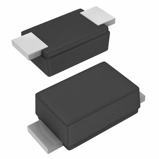
Part No.:
VTVS25ASMF-M3-18
Manufacturer:
Vishay General Semiconductor - Diodes Division
Category:
TVS Diodes
Package:
DO-219AB
Datasheet:
AetrixVTVS25ASMF-M3-18.pdf
Description:
TVS DIODE 25.2VWM 42VC DO219AB
Quantity:
Payment:
Payment
Shipping:
Shipping

Inventory:6,691

Please send an inquiry. Send us your inquiry, and we will respond immediately.

Part Number
Quantity*
Price
Name*
Company
Email*
Comments

Product details

Overview

VTVS25ASMF-M3-18 from Vishay Semiconductors is a unidirectional 400 W TransZorb® transient voltage suppressor diode in SMF (DO-219AB) package, designed for ESD and surge protection of low-voltage DC lines such as USB, HDMI, and automotive sensor interfaces. It features a 25.2 V maximum working voltage (VRWM), 28.5–31.5 V reverse breakdown voltage (VBR) at 1 mA, 42 A peak pulse current (IPPM) under 10/1000 μs waveform, and clamps to ≤42 V at rated current.

For engineers reviewing the VTVS25ASMF-M3-18 datasheet, VTVS25ASMF-M3-18 pinout, VTVS25ASMF-M3-18 application, or VTVS25ASMF-M3-18 equivalent, this device is selected for robust ±30 kV IEC 61000-4-2 contact/air discharge protection, low 433 pF capacitance at 0 V, and AEC-Q101 qualification suitability in space-constrained automotive and industrial PCB layouts.

Technical Context

The VTVS25ASMF-M3-18 operates as a unidirectional avalanche diode with precise 25.2 V stand-off capability and tight ±5 % VBR tolerance. Its low-clamping behavior (VC ≤ 42 V at IPPM = 9.07 A) ensures downstream IC protection during fast transients while maintaining signal integrity on high-speed lines.

Engineered for reflow and wave soldering, it uses halogen-free molding compound (UL 94 V-0), achieves MSL level 1 moisture sensitivity rating, and supports junction temperatures from –55 °C to +175 °C - enabling deployment in under-hood automotive environments and industrial control modules.

Key Specifications

Parameter Value and Actual Design Meaning
Peak Pulse Power 400 W (10/1000 μs waveform); sustains high-energy surges without thermal runaway
Stand-off Voltage (VRWM) 25.2 V max; defines maximum continuous DC operating voltage before leakage exceeds 0.05 μA
Breakdown Voltage (VBR) 28.5–31.5 V at IT = 1 mA; tight ±5 % tolerance enables predictable clamping onset
Clamping Voltage (VC) ≤42 V at IPPM = 9.07 A; limits transient overvoltage seen by protected ICs
Capacitance (CD) 433 pF at VR = 0 V, f = 1 MHz; low enough for USB 2.0 and CAN FD data lines
ESD Rating ±30 kV contact / ±30 kV air per IEC 61000-4-2; meets automotive infotainment ESD immunity requirements
Package SMF (DO-219AB); 3.9 × 1.9 × 1.08 mm footprint compatible with SOD-123W layout

Pinout & Package

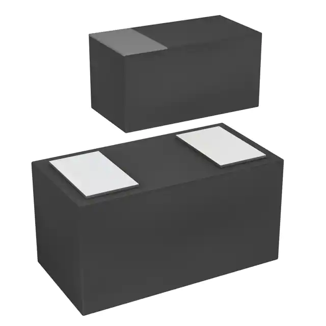
SMF (DO-219AB) package: surface-mount, low-profile (1.08 mm height), cathode marked by bar on top surface; compatible with standard SOD-123W PCB footprints and reflow profiles up to 260 °C peak.

Pin/Terminal Circuit Role Design Meaning
Anode Reference node for unidirectional clamping Connected to protected line's ground or low-side return path; defines polarity-sensitive protection direction
Cathode Transient current sink Connected to protected signal line; conducts surge current to ground when VR > VBR

Key Features

Feature Design Value
400 W peak pulse power Enables single-device protection against ISO 7637-2 pulse 1/2a/3a surges in 12 V automotive systems
±5 % VBR tolerance Reduces design margin uncertainty versus ±10 % parts, allowing tighter VRWM selection near IC absolute maximum ratings
433 pF capacitance Minimizes signal distortion on 480 Mbps USB 2.0 lines; avoids eye diagram closure or timing jitter
AEC-Q101 qualified Validated for automotive-grade reliability including temperature cycling, HTRB, and ESD stress per JESD22-A114
Halogen-free & RoHS-compliant Meets EU Directive 2011/65/EU and automotive OEM material declarations (e.g., GMW3172, Ford WSS-M99P9999-A1)

Applications

Automotive Sensor Interface USB 2.0 Port Protection

Use Scenario: Protecting LIN/CAN transceiver I/O pins and analog sensor outputs (e.g., pressure, temperature) in engine control units exposed to load dump and ISO 7637-2 pulses.

IC Role / Device Role: Unidirectional TVS diode placed between signal line and chassis ground to clamp transients before reaching sensitive analog front-end or transceiver inputs.

Use Value: Prevents latch-up or permanent damage to 3.3 V/5 V microcontrollers and ADCs during 12 V system surges, leveraging 25.2 V VRWM and 42 V VC clamping.

Use Scenario: Safeguarding D+ and D− lines of USB 2.0 host/device ports against ESD events in industrial HMIs and automotive infotainment head units.

IC Role / Device Role: Low-capacitance TVS placed differential across data lines to suppress ±30 kV contact discharge without degrading signal integrity.

Use Value: Maintains USB 2.0 eye diagram compliance (480 Mbps) with only 433 pF loading, avoiding bit errors or link renegotiation failures.

Industrial PLC Digital I/O Automotive Camera Module Power Line

Use Scenario: Protecting 24 V digital input channels on programmable logic controllers from field-induced surges and inductive switching transients.

IC Role / Device Role: Standoff-rated TVS connected between input terminal and common ground to absorb 400 W transients without forward conduction.

Use Value: Enables reliable operation in factory-floor environments with frequent relay coil switching, using 25.2 V VRWM to avoid false triggering on nominal 24 V signals.

Use Scenario: Shielding 12 V power supply lines feeding MIPI CSI-2 camera modules in ADAS systems from battery line transients and alternator ripple.

IC Role / Device Role: Unidirectional TVS installed between VCC and GND to clamp positive-going spikes while preserving quiescent current draw below 0.05 μA.

Use Value: Ensures camera module uptime during cold-crank and jump-start scenarios where VCC may spike to 30 V, leveraging 31.5 V VBR upper limit.

Equivalent & Alternatives

The following parts are listed as comparable options for similar transient voltage suppression applications.

Alternative Part Technical Difference Application Difference Selection Advice
SMAJ26A Higher VRWM (26 V), same DO-214AC package, but 400 W rating with looser ±10 % VBR tolerance Larger footprint (4.5 × 2.7 mm vs. 3.9 × 1.9 mm); less suitable for dense automotive PCBs Select when legacy SMA layout exists and tighter VBR tolerance is not required
TPSMF26A Same SMF package, 26 V VRWM, ±5 % VBR, but lower 200 W peak power (10/1000 μs) Insufficient for ISO 7637-2 pulse 1 (400 W requirement); limited to ESD-only use cases Choose only for cost-sensitive consumer electronics where 400 W surge immunity is not mandated

Compared with SMAJ26A and TPSMF26A, the VTVS25ASMF-M3-18 delivers superior space efficiency (30 % smaller footprint), tighter voltage tolerance for precision clamping, and full 400 W surge handling - making it optimal for next-generation automotive and industrial designs demanding miniaturization and robustness.

Availability

VTVS25ASMF-M3-18 is available at Aetrix Electronics and suitable for automotive sensor interfaces, USB 2.0 port protection, and industrial PLC digital I/O requiring stable component supply with AEC-Q101 assurance and traceable sourcing.

Supply support for VTVS25ASMF-M3-18 includes scheduled delivery planning, volume procurement assistance, BOM continuity management, traceable sourcing, and lifecycle availability coordination for OEM customers, industrial embedded developers, connected-device designers, and electronics production programs.

Manufacturer

Vishay Semiconductors is a global leader in discrete semiconductors, specializing in high-reliability diodes, MOSFETs, and optoelectronics for automotive, industrial, and computing markets.

The VTVS eSMP® Series targets compact, high-power transient suppression in harsh environments - engineered specifically for AEC-Q101 compliance, low-profile packaging, and consistent clamping performance across temperature.

FAQ

What is the maximum operating temperature range for the VTVS25ASMF-M3-18?

The VTVS25ASMF-M3-18 supports a junction temperature range of –55 °C to +175 °C, validated per AEC-Q101 stress testing. This allows direct placement in under-hood automotive locations and high-temperature industrial enclosures without derating, provided thermal resistance to ambient remains within RthJA limits specified in the datasheet.

Does the VTVS25ASMF-M3-18 meet automotive qualification standards?

Yes, the VTVS25ASMF-M3-18 is AEC-Q101 qualified, covering tests including HTGB, HTRB, temperature cycling, and ESD per JESD22-A114. The "M3" suffix denotes tape-and-reel packaging compliant with JEDEC J-STD-020 MSL level 1, and the "-18" indicates 10K per 13″ reel - both critical for automotive production traceability.

How does the 433 pF capacitance of the VTVS25ASMF-M3-18 affect high-speed signal lines?

The VTVS25ASMF-M3-18's 433 pF capacitance at 0 V is measured at 1 MHz and decreases significantly at higher bias voltages. On USB 2.0 D+/D− lines, this value introduces negligible insertion loss below 200 MHz, preserving eye diagram margins and ensuring interoperability with USB-IF certified hosts and peripherals without requiring additional equalization.

Can the VTVS25ASMF-M3-18 be used for bidirectional protection?

No, the VTVS25ASMF-M3-18 is a unidirectional TVS diode, optimized for clamping positive transients relative to ground. For bidirectional protection (e.g., AC lines or symmetric data buses), a dedicated bidirectional part such as VTVS25BSMF-M3-18 - with symmetrical ±25.2 V VRWM - must be selected instead.

What is the meaning of the "A" and "M3-18" in VTVS25ASMF-M3-18?

The "A" denotes ±5 % tolerance on reverse breakdown voltage (VBR); "M3" specifies halogen-free, RoHS-compliant, lead (Pb)-free terminations with tin plating; "-18" indicates packaging in 10K quantities per 13″ reel. These codes align with Vishay's standardized ordering nomenclature defined in document 85891 Rev. 2.2.

VTVS25ASMF-M3-18 Specifications

Product attributes
Attribute value
Manufacturer:
Vishay General Semiconductor - Diodes Division
Package/Case:
DO-219AB
Series:
TransZorb®
Packaging:
Tape & Reel (TR)
Product Status:
Active
Type:
Zener
Unidirectional Channels:
1
Bidirectional Channels:
-
Voltage - Reverse Standoff (Typ):
25.2V
Voltage - Breakdown (Min):
28.5V
Voltage - Clamping (Max) @ Ipp:
42V
Current - Peak Pulse (10/1000µs):
9.07A
Power - Peak Pulse:
400W
Power Line Protection:
No
Applications:
General Purpose
Capacitance @ Frequency:
433pF @ 1MHz
Operating Temperature:
-55°C ~ 175°C (TJ)
Grade:
-
Qualification:
-
Mounting Type:
Surface Mount
Supplier Device Package:
DO-219AB (SMF)

VTVS25ASMF-M3-18 FAQ

1.How can I place an order for VTVS25ASMF-M3-18 through Aetrix?

Please submit a Request for Quotation (RFQ) for VTVS25ASMF-M3-18 on Aetrix. Our sales agent will provide a competitive quotation and guide you through the order confirmation once you accept the terms.

2.Are the price and stock information for VTVS25ASMF-M3-18 reliable?

The price and inventory of VTVS25ASMF-M3-18 are updated periodically and may fluctuate due to market conditions. Stock and pricing data are typically refreshed every 24 hours. Quotation validity for VTVS25ASMF-M3-18 is usually 5 days.

3.What payment methods are accepted for VTVS25ASMF-M3-18?

We accept Wire Transfer, PayPal, Credit Card, Western Union, MoneyGram, and Escrow for VTVS25ASMF-M3-18 transactions.

Note: Certain payment methods may incur a processing fee.

4.How is shipping managed for VTVS25ASMF-M3-18?

VTVS25ASMF-M3-18 orders can be shipped via leading logistics carriers, including DHL, UPS, FedEx, TNT, or Registered Mail.

Once your VTVS25ASMF-M3-18 order is processed, you will receive an email with the shipment details and tracking number.

Note: Tracking information may take up to 24 hours to appear. Express delivery typically takes 3–5 business days.

5.How can I obtain technical support or documentation for VTVS25ASMF-M3-18?

For technical support, including VTVS25ASMF-M3-18 datasheets, pinout diagrams, or application guidance, please contact our engineering support team. They can provide detailed documentation and assistance for your VTVS25ASMF-M3-18 requirements.

6.How does Aetrix verify that VTVS25ASMF-M3-18 is sourced from the original manufacturer or authorized distributors?

All VTVS25ASMF-M3-18 products on Aetrix are procured from qualified distributors and authorized channels. Our dedicated quality assurance team conducts strict verification, including traceability checks and, if necessary, third-party testing. This ensures that VTVS25ASMF-M3-18 meets industry standards.

7.What is the process for return or replacement of VTVS25ASMF-M3-18?

All VTVS25ASMF-M3-18 units undergo pre-shipment inspection (PSI). If there is an issue with VTVS25ASMF-M3-18, returns or replacements are accepted under the following conditions:

1.Quantity discrepancies, incorrect items, or visible external defects (such as breakage or corrosion), acknowledged by Aetrix.

2.The issue is reported within 90 days of delivery.

3.The VTVS25ASMF-M3-18 part is unused and in its original packaging.

Return procedure for VTVS25ASMF-M3-18:

1.Submit a request within 90 days.

2.Obtain a Return Material Authorization (RMA) from Aetrix.

VTVS25ASMF-M3-18 Tags
  • VTVS25ASMF-M3-18
  • VTVS25ASMF-M3-18 PDF
  • VTVS25ASMF-M3-18 Datasheet
  • VTVS25ASMF-M3-18 Specifications
  • VTVS25ASMF-M3-18 Images
  • Vishay General Semiconductor - Diodes Division
  • Vishay General Semiconductor - Diodes Division VTVS25ASMF-M3-18
  • Buy VTVS25ASMF-M3-18
  • VTVS25ASMF-M3-18 Price
  • VTVS25ASMF-M3-18 Distributor
  • VTVS25ASMF-M3-18 Supplier
  • VTVS25ASMF-M3-18 Wholesale
Related Products
ESD9B5.0ST5G
ESD9B5.0ST5G

onsemi

DESD3V3E1BL-7B
DESD3V3E1BL-7B

Diodes Incorporated

ESD5Z3.3T1G
ESD5Z3.3T1G

onsemi

D5V0H1B2LP-7B
D5V0H1B2LP-7B

Diodes Incorporated

D5V0P1B2LP-7B
D5V0P1B2LP-7B

Diodes Incorporated

DESD5V0U1BA-7
DESD5V0U1BA-7

Diodes Incorporated

ESD5Z5.0T1G
ESD5Z5.0T1G

onsemi

DESD5V0U1BB-7
DESD5V0U1BB-7

Diodes Incorporated

D12V0L1B2LP-7B
D12V0L1B2LP-7B

Diodes Incorporated

PESD2V0Y1BSFYL
PESD2V0Y1BSFYL

Nexperia USA Inc.

DF2S5M4CT,L3F
DF2S5M4CT,L3F

Toshiba Semiconductor and Storage

D5V0L1B2WS-7
D5V0L1B2WS-7

Diodes Incorporated

Tech Hub
Search

Search

PRODUCT

PRODUCT

PHONE

PHONE

USER

USER