
 My Inquiry
 My Account


Diodes Incorporated ZNBG4008Q16TC
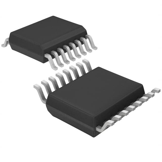
- Part No.:
- ZNBG4008Q16TC
- Manufacturer:
- Diodes Incorporated
- Category:
- Power Management - Specialized
- Package:
- 16-SSOP (0.154", 3.90mm Width)
- Datasheet:
-
 ZNBG4008Q16TC.pdf
- Description:
- IC SWITCH LNB BIAS 16QFN
- Quantity:
- Payment:

- Shipping:

Inventory:2,217
Please send an inquiry. Send us your inquiry, and we will respond immediately.
Product details
Overview
ZNBG4008Q16TC from Diodes Incorporated is a 4-stage GaAs/HEMT FET bias controller for satellite LNBs, providing regulated -3V gate bias and 2.2V drain supply per stage, with programmable 0–15mA drain current per FET group via RCAL1/RCAL2 resistors, operating from 5.0–12.0V single supply in QSOP-16 package.
For engineers reviewing the ZNBG4008Q16TC datasheet, ZNBG4008Q16TC pinout, ZNBG4008Q16TC application, or ZNBG4008Q16TC equivalent, this device delivers precise dual-group FET current control, integrated switched-capacitor negative rail generation, dynamic overcurrent protection, and temperature-stable drain voltage (±50 ppm/°C) for low-noise microwave front-end design.
Technical Context
The ZNBG4008Q16TC implements four independent bias stages grouped as (D1/G1, D3/G3) controlled by RCAL1 and (D2/G2, D4/G4) controlled by RCAL2, enabling noise-optimized input FETs and gain-optimized subsequent stages. Each stage features current-limited gate drivers and self-regulating drain supplies with ±0.2V tolerance at 2.2V nominal.
Its on-chip switched-capacitor DC-DC converter generates a regulated -3.0V substrate voltage (VCSUB) using two external 47nF capacitors (CNB, CSUB), with oscillator frequency ranging 200–800 kHz. Gate drive is clamped to -3.5V maximum under all conditions including power transients.
Key Specifications
| Parameter | Value and Actual Design Meaning |
|---|---|
| Supply Voltage Range | 4.5V to 12V - Enables direct use with standard LNB power injectors and avoids need for auxiliary regulators. |
| Drain Voltage (per stage) | 2.2V ±0.2V - Stable bias point for GaAs/HEMT FETs, minimizing gain drift across temperature (-40°C to +70°C). |
| Drain Current Range | 0–15mA per stage - Programmable via RCAL resistors to optimize noise (stages 1/3) or gain (stages 2/4). |
| Negative Rail Output | -3.0V ±0.5V - Internally generated, regulated substrate voltage for depletion-mode FET gate biasing. |
| Oscillator Frequency | 200–800 kHz - Sets switching frequency of integrated charge-pump; determines capacitor sizing and ripple performance. |
| Gate Noise Voltage | ≤5 mVpk-pk - Measured with 10nF gate/drain caps; critical for preserving LNB noise figure in RF front ends. |
| Thermal Drift (dVD/dTOP) | 50 ppm/°C - Ensures <±0.5% drain voltage variation over full operating range, supporting stable RF performance. |
Pinout & Package
Package: QSOP-16 (5.0 × 6.2 mm body, 0.635 mm pitch), lead-free, halogen-free, RoHS-compliant.
| Pin/Terminal | Circuit Role | Design Meaning |
|---|---|---|
| VDD | Positive Supply Input | Accepts 4.5–12V single supply; powers internal logic, oscillator, and charge pump. |
| G1–G4 | Gate Drive Outputs | Current-limited negative gate drivers (−3.5V max); each controls one grounded-source FET gate. |
| D1–D4 | Drain Supply Outputs | Regulated 2.2V outputs with per-stage current limiting; sink up to 15mA per FET drain. |
| RCAL1 / RCAL2 | Current Set Inputs | Resistor-to-ground sets drain current for FET pairs (1&3 or 2&4); enables dual optimization paths. |
| CSUB | Negative Rail Output | Provides regulated −3.0V for gate biasing and optional external circuits (mixers, LOs). |
| CNB | Charge Pump Capacitor | External 47nF capacitor for internal switched-capacitor DC-DC conversion. |
| GND | Ground Reference | Common return for VDD, CSUB, and all FET source connections. |
Key Features
| Feature | Design Value |
|---|---|
| Dual RCAL-controlled FET groups | RCAL1 sets ID for stages 1/3 (noise-critical input); RCAL2 sets ID for stages 2/4 (gain-critical amplification). |
| Integrated −3V charge-pump generator | Eliminates need for external negative supply; requires only two 47nF capacitors (CNB, CSUB). |
| Per-stage current limiting & fault shutdown | Each D-pin shuts down if its FET exceeds set current; CSUB fault disables all drains to prevent cascade failure. |
| Power-up/down gate voltage clamp | Guarantees gate drive never exceeds −3.5V during transients-protects sensitive GaAs/HEMT gates. |
| Low-noise bias regulation | ≤5 mVpk-pk gate noise and ≤20 mVpk-pk drain noise preserve LNB noise figure in Ku-band reception. |
Applications
| Direct Broadcast Satellite LNB | Twin/Quad LNB Modules |
|---|---|
|
Use Scenario: Biasing 4-stage GaAs FET amplifier chain in Ku-band satellite downconverters for residential dish antennas. IC Role / Device Role / Timing Role: Provides independent, low-noise gate and drain bias to each FET stage while generating required negative rail from single 13.5/18V LNB supply. Use Value: Enables >1dB NF improvement in first-stage FETs via optimized 5–8mA bias, while maintaining >15dB gain in later stages through 10–12mA settings. |
Use Scenario: Powering dual independent LNB paths (horizontal/vertical polarization) within single housing for multi-feed satellite receivers. IC Role / Device Role / Timing Role: Simultaneously regulates four FET stages across two polarization channels using shared VDD and separate RCAL networks. Use Value: Eliminates need for two discrete bias ICs; reduces PCB area by 40% and ensures matched inter-channel gain/noise performance. |
| Microwave Point-to-Point Links | PMR Base Station Front Ends |
|
Use Scenario: Stabilizing 10–12 GHz receiver front end in short-haul wireless backhaul equipment operating outdoors. IC Role / Device Role / Timing Role: Delivers thermally stable 2.2V drain voltage (50 ppm/°C drift) and −3.0V gate bias across −40°C to +70°C ambient. Use Value: Maintains <±0.3dB gain flatness and <±0.2dB NF shift over full temperature range-critical for link budget integrity. |
Use Scenario: Biasing low-noise amplifier stages in professional mobile radio (PMR) base station receivers (400–470 MHz). IC Role / Device Role / Timing Role: Supplies precision current-controlled bias to discrete HEMT devices in high-dynamic-range receive chains. Use Value: Supports >90dB spurious-free dynamic range (SFDR) by minimizing bias-induced intermodulation distortion in FETs. |
Equivalent & Alternatives
The following parts are listed as comparable options for similar FET bias controller applications.
| Alternative Part | Technical Difference | Application Difference | Selection Advice |
|---|---|---|---|
| ZNBG4004Q16TC | 2-stage version; identical architecture but half the channel count and lower ICC(max) = 30mA. | Suitable only for dual-FET LNBs or single-path systems; lacks RCAL2 and G3/G4/D3/D4 pins. | Select when biasing ≤2 FETs and board space or cost constraints preclude 4-stage solution. |
| MAX2641 | Single-stage 5V-only LNA bias IC with integrated 50Ω output matching; no negative rail generation. | Designed for monolithic MMIC biasing-not compatible with discrete GaAs/HEMT FETs requiring negative gate bias. | Choose only for 5V systems using matched MMICs; not a functional substitute for ZNBG4008Q16TC's multi-stage, negative-rail capability. |
Compared with ZNBG4004Q16TC, the ZNBG4008Q16TC supports full quad-LNB architectures and dual-optimization biasing; versus MAX2641, it uniquely provides regulated negative gate voltage and multi-stage current control essential for discrete FET front ends.
Availability
ZNBG4008Q16TC is available at Aetrix Electronics and suitable for satellite LNB modules, microwave point-to-point links, and PMR base station receivers requiring stable component supply, consistent thermal performance, and RoHS-compliant packaging.
Supply support for ZNBG4008Q16TC includes scheduled delivery planning, volume procurement assistance, BOM continuity management, traceable sourcing, and lifecycle availability coordination for OEM customers, industrial embedded developers, connected-device designers, and electronics production programs.
Manufacturer
Diodes Incorporated is a global manufacturer of discrete semiconductors and analog ICs, specializing in high-reliability power management, signal integrity, and precision timing solutions for industrial, automotive, and communications markets.
The ZNBG series targets satellite receiver infrastructure, delivering minimal-component FET bias control with integrated negative rail generation-designed specifically for LNB manufacturers needing robust, temperature-stable, and ESD-hardened bias solutions.
FAQ
What external components are mandatory for ZNBG4008Q16TC operation?
Two 47nF ceramic capacitors (CNB and CSUB) are mandatory for the internal charge-pump negative rail generation. RCAL1 and RCAL2 resistors are required to set drain currents-omitting either disables its associated FET pair. No additional passive components are needed for basic bias functionality.
Can unused bias stages be left unconnected without affecting performance?
Yes. Unused Gx and Dx pins may be left open-circuit with no impact on remaining stages. If an entire RCAL group (e.g., RCAL2) is unused, its resistor may be omitted. The IC automatically isolates inactive sections, maintaining regulation accuracy and noise performance on active channels.
How does the ZNBG4008Q16TC protect external FETs during power-up?
It enforces strict gate voltage limits: gate drivers never exceed −3.5V under any condition, including cold-start or rapid VDD ramp. Each drain output has independent current limiting, and the CSUB rail shuts down entirely if overloaded-preventing destructive current surges into sensitive GaAs/HEMT devices.
Is the −3V CSUB output capable of powering external circuitry?
Yes. The CSUB pin delivers up to 20mA of regulated −3.0V current and is explicitly intended for external use-such as biasing mixers, local oscillators, or additional discrete FET stages-provided total load remains within the charge-pump's capability and noise requirements are met.
ZNBG4008Q16TC Specifications
- Product attributes
- Attribute value
- Manufacturer:
- Diodes Incorporated
- Series:
- -
- Package/Case:
- 16-SSOP (0.154", 3.90mm Width)
- Packaging:
- Tape & Reel (TR)
- Product Status:
- Obsolete
- Applications:
- Bias Controller
- Current - Supply:
- 50mA
- Voltage - Supply:
- 4.5V ~ 12V
- Operating Temperature:
- -40°C ~ 70°C (TA)
- Grade:
- -
- Qualification:
- -
- Mounting Type:
- Surface Mount
- Supplier Device Package:
- 16-QSOP
ZNBG4008Q16TC FAQ
1.How can I place an order for ZNBG4008Q16TC through Aetrix?
Please submit a Request for Quotation (RFQ) for ZNBG4008Q16TC on Aetrix. Our sales agent will provide a competitive quotation and guide you through the order confirmation once you accept the terms.
2.Are the price and stock information for ZNBG4008Q16TC reliable?
The price and inventory of ZNBG4008Q16TC are updated periodically and may fluctuate due to market conditions. Stock and pricing data are typically refreshed every 24 hours. Quotation validity for ZNBG4008Q16TC is usually 5 days.
3.What payment methods are accepted for ZNBG4008Q16TC?
We accept Wire Transfer, PayPal, Credit Card, Western Union, MoneyGram, and Escrow for ZNBG4008Q16TC transactions.
Note: Certain payment methods may incur a processing fee.
4.How is shipping managed for ZNBG4008Q16TC?
ZNBG4008Q16TC orders can be shipped via leading logistics carriers, including DHL, UPS, FedEx, TNT, or Registered Mail.
Once your ZNBG4008Q16TC order is processed, you will receive an email with the shipment details and tracking number.
Note: Tracking information may take up to 24 hours to appear. Express delivery typically takes 3–5 business days.
5.How can I obtain technical support or documentation for ZNBG4008Q16TC?
For technical support, including ZNBG4008Q16TC datasheets, pinout diagrams, or application guidance, please contact our engineering support team. They can provide detailed documentation and assistance for your ZNBG4008Q16TC requirements.
6.How does Aetrix verify that ZNBG4008Q16TC is sourced from the original manufacturer or authorized distributors?
All ZNBG4008Q16TC products on Aetrix are procured from qualified distributors and authorized channels. Our dedicated quality assurance team conducts strict verification, including traceability checks and, if necessary, third-party testing. This ensures that ZNBG4008Q16TC meets industry standards.
7.What is the process for return or replacement of ZNBG4008Q16TC?
All ZNBG4008Q16TC units undergo pre-shipment inspection (PSI). If there is an issue with ZNBG4008Q16TC, returns or replacements are accepted under the following conditions:
1.Quantity discrepancies, incorrect items, or visible external defects (such as breakage or corrosion), acknowledged by Aetrix.
2.The issue is reported within 90 days of delivery.
3.The ZNBG4008Q16TC part is unused and in its original packaging.
Return procedure for ZNBG4008Q16TC:
1.Submit a request within 90 days.
2.Obtain a Return Material Authorization (RMA) from Aetrix.
ZNBG4008Q16TC Tags

-
TPS2511DGNR
Texas Instruments

-
UTC2000/MG
Microchip Technology

-
TUSB320HAIRWBR
Texas Instruments

-
TPS61252DSGR
Texas Instruments

-
PI5USB30216CXUAEX
Diodes Incorporated

-
SN6501DBVR
Texas Instruments

-
CYPD3177-24LQXQT
Infineon Technologies
-
SN6501QDBVRQ1
Texas Instruments

-
STUSB1600AQTR
STMicroelectronics

-
SN6505BDBVR
Texas Instruments
-
SN6501DBVT
Texas Instruments

-
TPS65150PWPR
Texas Instruments
Tech Hub

An engineering guide to LED driver operation, constant-current and constant-voltage outputs, linear and switching topologies, dimming, IC selection, calculations, replacement compatibility, and fault c…

Operational amplifier guide covering op amp basics, feedback, ideal vs real op amps, common configurations, buffer circuits, offset, bias current, gain-bandwidth, slew rate, rail-to-rail limits and sel…

Jumper cables guide covering safe connection order, red and black clamp placement, final ground connection, cable gauge, length, clamp quality, copper vs CCA cables, jump starter comparison and battery…

LDO regulator guide covering low dropout voltage, power dissipation, thermal design, PSRR, output noise, capacitor stability, adjustable LDO circuits, LDO vs buck converter and datasheet selection chec…

Conditional Access Module guide covering CAM meaning, CI/CI+ interface, smart card authorization, DVB security workflow, TV and set-top box compatibility, internal electronics, ESD protection, connecto…

Guide to electronic component obsolescence covering EOL risk, PCN/PDN notices, last-time buy planning, replacement options, form-fit-function validation, counterfeit risk and BOM lifecycle management.

18650 battery guide covering lithium-ion cell basics, 3.6V/3.7V voltage, 4.2V charging, mAh and Wh capacity, protected cells, chargers, BMS, series-parallel packs, holders, welding and sourcing checks.…

Hall effect sensor guide covering working principle, linear and digital sensors, Arduino circuits, current sensing, speed detection, automotive applications, A3144 examples, signal filtering and datash…

Product Change Notification guide for electronic components, covering PCN meaning, PCN vs PDN/EOL, common change types, risk levels, form-fit-function review, engineering validation, BOM control, LTB/L…

A practical guide to blend door actuators, covering HVAC function, symptoms, location, AC and heater issues, reset and calibration, replacement cost, electrical diagnosis, compatibility checks, and rep…


