
 My Inquiry
 My Account


Analog Devices Inc. ADXL362BCCZ-MI-RL7
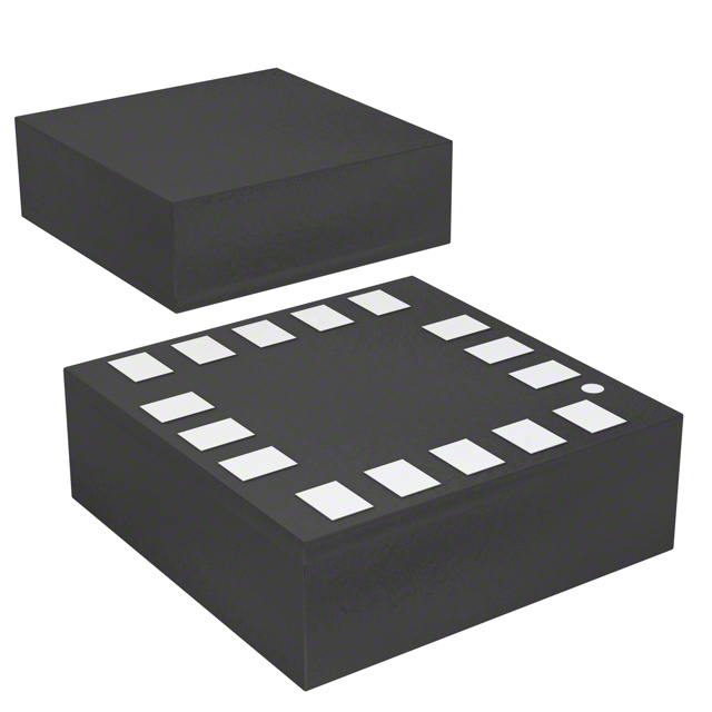
- Part No.:
- ADXL362BCCZ-MI-RL7
- Manufacturer:
- Analog Devices Inc.
- Category:
- Accelerometers
- Package:
- 16-TFLGA
- Datasheet:
-
 ADXL362BCCZ-MI-RL7.pdf
- Description:
- ACCELEROMETER 2-8G SPI 16LGA
- Quantity:
- Payment:

- Shipping:

Inventory:2,856
Please send an inquiry. Send us your inquiry, and we will respond immediately.
Product details
Overview
ADXL362BCCZ-MI-RL7 from Analog Devices is an ultralow-power, 3-axis MEMS accelerometer with ±2 g/±4 g/±8 g selectable ranges, 12-bit resolution (1 mg/LSB on ±2 g), SPI interface, and true continuous sampling-no undersampling or aliasing. It operates from 1.6 V to 3.5 V, draws only 1.8 µA at 100 Hz ODR, and supports motion-triggered wake-up at 270 nA for battery-powered hearing aids and wireless sensors.
For engineers reviewing the ADXL362BCCZ-MI-RL7 datasheet, ADXL362BCCZ-MI-RL7 pinout, ADXL362BCCZ-MI-RL7 application, or ADXL362BCCZ-MI-RL7 equivalent, key selection criteria include guaranteed 12-bit output resolution across all ODRs, autonomous interrupt generation without MCU involvement, deep FIFO for burst data capture, low-noise modes down to 175 µg/√Hz, and integrated temperature sensor with 0.065 °C/LSB sensitivity.
Technical Context
The ADXL362BCCZ-MI-RL7 uses a polysilicon surface-micromachined capacitive sensing element with phase-sensitive demodulation, enabling true static (tilt) and dynamic acceleration measurement. Its digital architecture includes a 12-bit ADC, configurable antialiasing filter (½ or ¼ ODR), and autonomous activity/inactivity detection logic that operates independently of host intervention.
It implements three distinct power states: measurement mode (≤3.0 µA at 400 Hz), wake-up mode (270 nA at ~6 Hz activity check), and standby (10 nA). All modes retain register access and FIFO functionality except the activity timer in wake-up mode, and all support SPI communication and external trigger synchronization.
Key Specifications
| Parameter | Value and Actual Design Meaning |
|---|---|
| Output Data Rate | 12.5–400 Hz user-selectable; enables precise tradeoff between latency and power without aliasing. |
| Power Consumption | 1.8 µA typical at 100 Hz / 2.0 V; allows >1-year operation on CR2032 coin cell in continuous monitoring. |
| Resolution & Sensitivity | 12-bit output; 1 mg/LSB on ±2 g range-enables sub-degree tilt resolution in portable healthcare devices. |
| Noise Density | 175 µg/√Hz in ultra-low-noise mode at 3.5 V-supports high-fidelity vibration analysis in low-amplitude applications. |
| Supply Range | 1.6 V to 3.5 V; I/O compatible with 1.6–3.3 V hosts-eliminates level-shifting in mixed-voltage embedded systems. |
| Temperature Sensor | On-chip, 12-bit, 0.065 °C/LSB sensitivity-provides calibrated thermal compensation without external components. |
| FIFO Depth | 512 × 16-bit entries-reduces host polling frequency and enables burst-mode data acquisition. |
Pinout & Package
ADXL362BCCZ-MI-RL7 is housed in a 3 mm × 3.25 mm × 1.06 mm, 16-terminal LGA package with exposed pad (θJA = 150°C/W). Pin 1 is marked with "•362B" on top surface; pins 2, 15 are NC; pins 3, 5, 10 are reserved (GND optional); pins 12, 13, 16 are GND; pin 14 is VS.
| Pin/Terminal | Circuit Role | Design Meaning |
|---|---|---|
| VDD I/O (Pin 1) | Digital I/O supply rail | Independent from analog VS; allows interfacing with lower-voltage microcontrollers (1.6–3.3 V). |
| SCLK (Pin 4) | SPI clock input | Supports up to 5 MHz SCLK; timing-critical for deterministic interrupt latency and synchronized sampling. |
| MOSI (Pin 6) | SPI data input | Used for register writes, configuration commands, and self-test activation. |
| MISO (Pin 7) | SPI data output | Provides 16-bit aligned acceleration data, status flags, FIFO entries, and temperature readings. |
| CS (Pin 8) | SPI chip select (active low) | Enables multi-device SPI bus sharing; must be held low for entire transaction (min 50 ns pulse width). |
| INT1 (Pin 11) | Interrupt 1 output / external clock input | Configurable as motion-triggered wake signal or external timing reference for synchronized sampling. |
| INT2 (Pin 9) | Interrupt 2 output / sync trigger input | Supports dual-interrupt event handling (e.g., activity + FIFO full) or external sampling alignment. |
| VS (Pin 14) | Analog supply voltage | 1.6–3.5 V range powers sensor core and ADC; noise on VS directly impacts noise density and PSRR. |
Key Features
| Feature | Design Value |
|---|---|
| Autonomous motion detection | Adjustable threshold and time window for activity/inactivity; runs at 270 nA without MCU-enables zero-power system sleep. |
| Deep multimode FIFO | 512-entry buffer with watermark and overrun detection; reduces host processor wake-ups by >90% in intermittent sensing. |
| True continuous sampling | No duty cycling or undersampling-full sensor bandwidth sampled at all ODRs, eliminating aliasing artifacts in vibration diagnostics. |
| Awake-state output pin | Dedicated AWAKE signal indicates real-time motion status; drives external load switches directly for standalone motion-activated power control. |
| Configurable low-noise modes | Two selectable modes (400 µg/√Hz and 250 µg/√Hz at 2.0 V) with <2× current increase-preserves battery life while enhancing SNR. |
Applications
| Hearing Aid Motion Control | Home Healthcare Monitoring |
|---|---|
Use Scenario: Real-time head movement detection during speech enhancement processing in wearable hearing aids. IC Role / Device Role / Timing Role: Primary motion sensor providing tilt and gesture data to DSP engine; outputs synchronized samples via INT2 trigger. Use Value: Enables adaptive beamforming and wind-noise suppression using 12-bit, 100 Hz ODR data with <1.8 µA draw-extending CR2032 battery life beyond 18 months. | Use Scenario: Fall detection and activity logging in portable ECG or respiratory monitors worn by elderly patients. IC Role / Device Role / Timing Role: System-level wake controller; triggers full-sensor acquisition only upon sustained acceleration exceeding 0.5 g for ≥500 ms. Use Value: Reduces average system current to <500 nA during idle-achieving multi-year operation on single AA alkaline cell. |
| Wireless Industrial Sensor Node | Motion-Enabled Utility Meter |
Use Scenario: Vibration signature capture in predictive maintenance nodes deployed on motors or pumps. IC Role / Device Role / Timing Role: High-fidelity acceleration front-end; uses ultra-low-noise mode (175 µg/√Hz) and external clock sync for phase-coherent multi-node measurements. Use Value: Delivers FFT-ready data at 400 Hz with <3 µA consumption-enabling 10-year mesh network lifetime without battery replacement. | Use Scenario: Tamper detection and usage pattern analysis in smart water/gas meters installed in unpowered locations. IC Role / Device Role / Timing Role: Always-on motion sentinel; asserts INT1 to wake meter SoC only when enclosure movement exceeds calibrated threshold. Use Value: Eliminates false alarms from ambient vibration via referenced activity detection-reducing unnecessary RF transmissions by >95%. |
Equivalent & Alternatives
The following parts are listed as comparable options for similar 3-axis micropower accelerometer applications.
| Alternative Part | Technical Difference | Application Difference | Selection Advice |
|---|---|---|---|
| ADXL372BCCZ-RL7 | Higher full-scale range (±200 g), lower resolution (12-bit but 12.5 mg/LSB), optimized for shock detection-not tilt or low-g motion. | Targeted at impact monitoring (e.g., drop testing), not healthcare or motion-switching. | Select only if measuring high-g transients; incompatible for sub-1 g applications like fall detection. |
| LSM6DSOXTR | Integrated 6-DoF IMU (gyro + accel), higher current (150 µA typical), no 270 nA wake-up mode, different SPI timing. | Requires full-system wake for any motion event; lacks autonomous low-power decision logic. | Choose when gyro data is essential; avoid if battery life >5 years or true autonomous wake-up is required. |
Compared with ADXL362BCCZ-MI-RL7, ADXL372BCCZ-RL7 trades low-g sensitivity for high-g robustness, while LSM6DSOXTR adds gyro functionality at 80× higher wake-current cost-making ADXL362BCCZ-MI-RL7 uniquely suited for ultra-long-life, motion-triggered, low-g sensing where autonomous decision-making is critical.
Availability
ADXL362BCCZ-MI-RL7 is available at Aetrix Electronics and suitable for hearing aid design, home healthcare device integration, and wireless sensor node development requiring stable component supply, long-term lifecycle assurance, and traceable sourcing.
Supply support for ADXL362BCCZ-MI-RL7 includes scheduled delivery planning, volume procurement assistance, BOM continuity management, traceable sourcing, and lifecycle availability coordination for OEM customers, industrial embedded developers, connected-device designers, and electronics production programs.
Manufacturer
Analog Devices is a global semiconductor leader specializing in high-performance analog, mixed-signal, and digital signal processing technologies for precision sensing, power management, and connectivity.
The ADXL362 product line was designed specifically for ultra-low-power, always-on motion sensing in battery-constrained applications-emphasizing autonomous operation, minimal system-level intervention, and guaranteed performance across extended temperature and voltage ranges.
FAQ
What is the guaranteed minimum output data rate for ADXL362BCCZ-MI-RL7?
The ADXL362BCCZ-MI-RL7 guarantees a minimum output data rate of 12.5 Hz across its full operating temperature range (−40°C to +85°C) and supply voltage range (1.6 V to 3.5 V). This rate is achieved with HALF_BW = 0 and is fully supported in both measurement and wake-up modes, enabling reliable low-frequency motion tracking in sleep-state monitoring applications without aliasing.
Does ADXL362BCCZ-MI-RL7 support I²C interface?
No, ADXL362BCCZ-MI-RL7 supports SPI only-specifically a 4-wire interface (SCLK, MOSI, MISO, CS) with no I²C capability. The device requires active chip select assertion and supports multi-byte transfers with address auto-increment. I²C users must select alternative accelerometers such as the ADXL345 or ICM-20689.
Can ADXL362BCCZ-MI-RL7 operate from a 1.6 V supply while maintaining full 12-bit resolution?
Yes, ADXL362BCCZ-MI-RL7 maintains full 12-bit output resolution and specified noise performance (550 µg/√Hz typical) at 1.6 V supply. All registers, FIFO, interrupt logic, and temperature sensor remain fully functional. Current consumption increases slightly to ~2.0 µA at 100 Hz ODR, but remains within datasheet limits and retains compatibility with coin-cell and energy-harvesting sources.
How does the referenced activity detection mode work in ADXL362BCCZ-MI-RL7?
In referenced activity mode, ADXL362BCCZ-MI-RL7 calculates a dynamic baseline from initial stationary orientation, then detects motion only when acceleration deviates by more than a user-defined threshold from that baseline (|Acc − Reference| > Threshold). This eliminates false triggers from gravity (1 g static offset), making it ideal for tilt-insensitive motion switches in handheld medical devices where orientation varies.
Is the ADXL362BCCZ-MI-RL7 RoHS compliant and lead-free?
Yes, ADXL362BCCZ-MI-RL7 is RoHS compliant and lead-free. The package branding includes a "#" prefix (e.g., #yww in Table 4), indicating Pb-free construction per JEDEC J-STD-609. The device meets Analog Devices' environmental compliance standards, including exemption 7a for lead in high-melting-temperature solder alloys, and ships with standard SnAgCu (SAC305) finish.
ADXL362BCCZ-MI-RL7 Specifications
- Product attributes
- Attribute value
- Manufacturer:
- Analog Devices Inc.
- Series:
- -
- Package/Case:
- 16-TFLGA
- Packaging:
- Tape & Reel (TR)
- Product Status:
- Active
- Type:
- Digital
- Axis:
- X, Y, Z
- Acceleration Range:
- ±2g, 4g, 8g
- Sensitivity (LSB/g):
- 1 (±2g) ~ 4 (±8g)
- Sensitivity (mV/g):
- -
- Bandwidth:
- 6.25Hz ~ 400Hz
- Output Type:
- SPI
- Voltage - Supply:
- 1.6V ~ 3.5V
- Features:
- Sleep Mode, Temperature Sensor
- Operating Temperature:
- -40°C ~ 85°C
- Grade:
- -
- Qualification:
- -
- Mounting Type:
- Surface Mount
- Supplier Device Package:
- 16-LGA (3x3.25)
ADXL362BCCZ-MI-RL7 FAQ
1.How can I place an order for ADXL362BCCZ-MI-RL7 through Aetrix?
Please submit a Request for Quotation (RFQ) for ADXL362BCCZ-MI-RL7 on Aetrix. Our sales agent will provide a competitive quotation and guide you through the order confirmation once you accept the terms.
2.Are the price and stock information for ADXL362BCCZ-MI-RL7 reliable?
The price and inventory of ADXL362BCCZ-MI-RL7 are updated periodically and may fluctuate due to market conditions. Stock and pricing data are typically refreshed every 24 hours. Quotation validity for ADXL362BCCZ-MI-RL7 is usually 5 days.
3.What payment methods are accepted for ADXL362BCCZ-MI-RL7?
We accept Wire Transfer, PayPal, Credit Card, Western Union, MoneyGram, and Escrow for ADXL362BCCZ-MI-RL7 transactions.
Note: Certain payment methods may incur a processing fee.
4.How is shipping managed for ADXL362BCCZ-MI-RL7?
ADXL362BCCZ-MI-RL7 orders can be shipped via leading logistics carriers, including DHL, UPS, FedEx, TNT, or Registered Mail.
Once your ADXL362BCCZ-MI-RL7 order is processed, you will receive an email with the shipment details and tracking number.
Note: Tracking information may take up to 24 hours to appear. Express delivery typically takes 3–5 business days.
5.How can I obtain technical support or documentation for ADXL362BCCZ-MI-RL7?
For technical support, including ADXL362BCCZ-MI-RL7 datasheets, pinout diagrams, or application guidance, please contact our engineering support team. They can provide detailed documentation and assistance for your ADXL362BCCZ-MI-RL7 requirements.
6.How does Aetrix verify that ADXL362BCCZ-MI-RL7 is sourced from the original manufacturer or authorized distributors?
All ADXL362BCCZ-MI-RL7 products on Aetrix are procured from qualified distributors and authorized channels. Our dedicated quality assurance team conducts strict verification, including traceability checks and, if necessary, third-party testing. This ensures that ADXL362BCCZ-MI-RL7 meets industry standards.
7.What is the process for return or replacement of ADXL362BCCZ-MI-RL7?
All ADXL362BCCZ-MI-RL7 units undergo pre-shipment inspection (PSI). If there is an issue with ADXL362BCCZ-MI-RL7, returns or replacements are accepted under the following conditions:
1.Quantity discrepancies, incorrect items, or visible external defects (such as breakage or corrosion), acknowledged by Aetrix.
2.The issue is reported within 90 days of delivery.
3.The ADXL362BCCZ-MI-RL7 part is unused and in its original packaging.
Return procedure for ADXL362BCCZ-MI-RL7:
1.Submit a request within 90 days.
2.Obtain a Return Material Authorization (RMA) from Aetrix.
ADXL362BCCZ-MI-RL7 Tags

-
MXC4005XC
Memsic Inc.

-
MC3419
Memsic Inc.

-
MC3479
Memsic Inc.

-
MXC6655XA
Memsic Inc.

-
MC3630
Memsic Inc.
.jpg)
-
LIS2HH12TR
STMicroelectronics

-
KX122-1037
Kionix Inc.
-
LIS2DE12TR
STMicroelectronics
-
LIS2DH12TR
STMicroelectronics

-
MC3635
Memsic Inc.
-
LIS2DS12TR
STMicroelectronics

-
LIS3DHTR
STMicroelectronics
Tech Hub

A practical engineering guide to 3.3V and 5V logic compatibility, input thresholds, resistor dividers, translator ICs, MOSFET level shifting, I2C pull-ups, timing limits and power-sequencing risks.

The 74HC595 uses push-pull logic outputs, while the TPIC6B595 uses 50 V open-drain DMOS sinks for higher-power loads. This guide compares timing, current limits, 3.3 V interfacing, load wiring, thermal…

The 74HC595 converts serial data into eight stable parallel outputs. This guide covers pin functions, shift and storage timing, OE and MR behavior, drive-current limits, cascading, voltage compatibilit…

A technical comparison of level-sensitive latches and edge-triggered flip-flops, covering timing windows, setup and hold limits, master–slave operation, time borrowing, race-through, HDL inference and…

A D latch stores one bit while Enable controls when data can pass. This reference covers gate-level operation, truth tables, transparency, setup and hold timing, LE versus OE, common ICs and practical …

An SR latch stores one bit through cross-coupled feedback. This engineering reference covers NOR and NAND implementations, truth tables, forbidden-state recovery, gated operation, switch debouncing, fa…

Latch circuits retain one bit through feedback. This technical reference covers SR and D latches, truth tables, transparency, timing limits, latch-versus-flip-flop behavior, applications and common log…

An engineering guide to LED driver operation, constant-current and constant-voltage outputs, linear and switching topologies, dimming, IC selection, calculations, replacement compatibility, and fault c…

Operational amplifier guide covering op amp basics, feedback, ideal vs real op amps, common configurations, buffer circuits, offset, bias current, gain-bandwidth, slew rate, rail-to-rail limits and sel…

Jumper cables guide covering safe connection order, red and black clamp placement, final ground connection, cable gauge, length, clamp quality, copper vs CCA cables, jump starter comparison and battery…


