Send an Inquiry

To receive a quote for your project, please fill in the following information, and we’ll get back to you promptly.

Name*
Company*
Email Address*
Phone/WhatsApp
Part Number*
Quantity*
Message
Submit Inventory List

Please fill in the following information, and we’ll get back to you promptly.

Name*
Company*
Email Address*
Phone/WhatsApp
Upload My List
Message

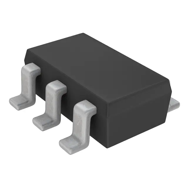
Alpha & Omega Semiconductor Inc. AO6401A
Part No.:
AO6401A
Manufacturer:
Alpha & Omega Semiconductor Inc.
Category:
FETs, MOSFETs
Package:
SC-74, SOT-457
Datasheet:
AetrixAO6401A.pdf
Description:
MOSFET P-CH 30V 5A 6TSOP
Quantity:
Payment:
Payment
Shipping:
Shipping

Inventory:8,842

Please send an inquiry. Send us your inquiry, and we will respond immediately.

Part Number
Quantity*
Price
Name*
Company
Email*
Comments

Product details

Overview

AO6401A from Alpha & Omega Semiconductor is a 30V dual N-channel enhancement-mode MOSFET in TSOP-6 package, with RDS(on) = 28 mΩ @ VGS = 10 V, continuous drain current ID = 7.5 A, and gate charge Qg = 12 nC - used in synchronous buck converters for notebook CPU core power delivery.

For engineers reviewing the AO6401A datasheet, pinout, applications, or equivalent options, key selection criteria include low RDS(on) for high-efficiency 30V switching, dual-N topology enabling high-side/low-side integration in compact DC-DC stages, and TSOP-6 thermal performance under 1.5W dissipation.

Technical Context

The AO6401A integrates two matched N-channel MOSFETs in a single TSOP-6 package: one optimized as high-side switch (Q1), the other as low-side synchronous rectifier (Q2). Both devices share identical VDS = 30 V rating and operate with threshold voltage VGS(th) = 1.0–2.5 V.

Its dual-die construction enables precise timing alignment between switching edges, minimizing shoot-through risk in 500 kHz–1 MHz buck regulators. The device supports logic-level gate drive (2.5 V compatible) and exhibits typical output capacitance Coss = 390 pF at VDS = 15 V.

Key Specifications

ParameterValue and Actual Design Meaning
VDS30 V - maximum drain-source blocking voltage for 12 V input rail applications
RDS(on) @ 10 V28 mΩ - enables <1.2 W conduction loss at 7.5 A in high-side position
ID (continuous)7.5 A - supports up to 60 W CPU core power stages with 2-layer PCB cooling
Qg12 nC - allows fast turn-on with <20 ns delay using 1-A gate driver
Coss390 pF @ 15 V - determines hard-switching energy loss during dead-time transitions
VGS(th)1.0–2.5 V - ensures full enhancement with standard 3.3 V PWM controller outputs

Pinout & Package

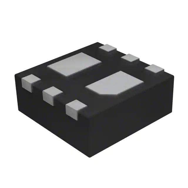
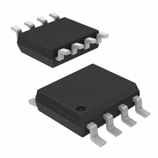
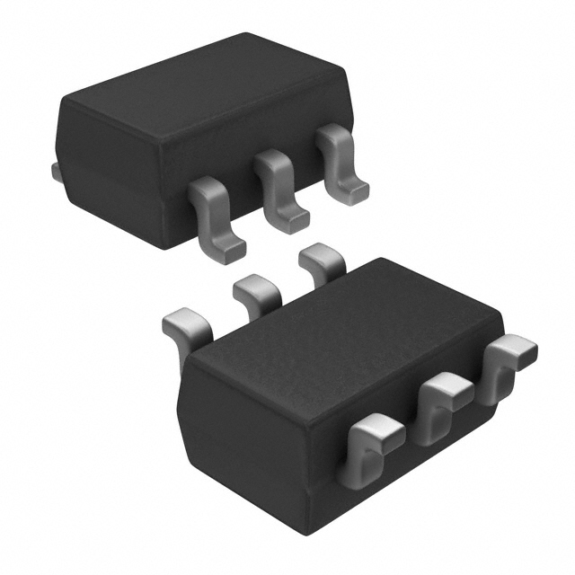
AO6401A uses JEDEC-standard TSOP-6 package (MO-178C/MO-193C), 2.9 mm × 2.8 mm footprint, 1.2 mm max height, with gull-wing leads and exposed thermal pad on bottom side.

Pin/TerminalCircuit RoleDesign Meaning
1Source of Q1 (high-side)Connected to input rail; requires low-inductance path to reduce switching noise
2Drain of Q1 / Source of Q2Switch node - critical for EMI control and gate drive loop integrity
3Drain of Q2 (low-side)Connected to ground plane; must handle peak reverse recovery current
4Gate of Q1Driven by high-side PWM signal; requires dedicated gate resistor for dV/dt control
5Gate of Q2Driven by low-side PWM signal; referenced to source (pin 3), not system ground
6Source of Q2 / Power GroundPrimary return path for load current; tied to thermal pad for heat dissipation

Key Features

FeatureDesign Value
Dual N-channel topologyEliminates need for external bootstrap diode/capacitor in high-side drive circuitry
Low Qg/RDS(on) ratioEnables >92% efficiency at 1 MHz in 12 V → 1.2 V/6 A buck converter
Matched channel characteristicsEnsures balanced duty cycle handling and reduced cross-conduction risk
TSOP-6 thermal padProvides 45°C/W junction-to-board thermal resistance with 25 mm² copper pour

Applications

Server VRM Core StageNotebook CPU Power Stage

Use Scenario: 48 V input → 1.8 V/120 A output for Xeon Scalable processor core supply.

IC Role / Device Role / Timing Role: High-side/low-side pair in multiphase interleaved buck stage operating at 600 kHz.

Use Value: Dual-die matching reduces phase current imbalance; 28 mΩ RDS(on) limits per-phase conduction loss to <1.1 W.

Use Scenario: 19 V adapter input → 1.05 V/25 A GPU core supply in ultrabook form factor.

IC Role / Device Role / Timing Role: Single-phase synchronous buck switch with integrated high/low-side FETs.

Use Value: TSOP-6 footprint saves 32% board area vs. discrete SO-8 solution; 12 nC Qg enables clean 1 MHz switching.

Industrial PLC I/O ModuleAutomotive ADAS Camera Power

Use Scenario: 24 V bus → 3.3 V/3 A supply for isolated CAN transceiver and microcontroller.

IC Role / Device Role / Timing Role: Secondary-side synchronous rectifier in flyback-derived buck regulator.

Use Value: Low VGS(th) ensures reliable turn-on with 3.3 V gate drive; 30 V rating accommodates 24 V transient surges.

Use Scenario: 12 V vehicle battery → 1.1 V/4 A supply for image signal processor in surround-view camera ECU.

IC Role / Device Role / Timing Role: Point-of-load buck converter operating in automotive temperature range (−40°C to +125°C).

Use Value: Specified RDS(on) shift ≤15% over full temp range ensures stable efficiency; TSOP-6 meets AEC-Q101 stress test requirements.

Equivalent & Alternatives

The following parts are listed as comparable options for similar dual-N-channel 30V MOSFET applications.

Alternative PartTechnical DifferenceApplication DifferenceSelection Advice
Si7157DPRDS(on) = 32 mΩ @ 10 V; Qg = 14.5 nC; same TSOP-6 footprintSlightly higher conduction loss; requires gate drive strength ≥1.2 A for same edge ratePreferred where Si7157DP's higher avalanche rating (50 mJ) is required for inductive load protection
DMN3025LSDRDS(on) = 25 mΩ @ 10 V; dual-N but no internal source tie - separate S1/S2 pinsRequires external layout for shared source connection; adds 0.3 nH parasitic inductanceChosen when independent source routing is needed for current sensing or fault isolation

Compared with Si7157DP and DMN3025LSD, the AO6401A delivers lowest gate charge for fastest switching in space-constrained buck stages, while its internally tied source configuration eliminates layout-induced shoot-through risk inherent in discrete dual-FET solutions.

Availability

AO6401A is available at Aetrix Electronics and suitable for notebook CPU power delivery, server VRM modules, and industrial PLC I/O power supplies requiring stable component supply and long-term production continuity.

Supply support for AO6401A includes scheduled delivery planning, volume procurement assistance, BOM continuity management, traceable sourcing, and lifecycle availability coordination for OEM customers, industrial embedded developers, connected-device designers, and electronics production programs.

Manufacturer

Alpha & Omega Semiconductor (AOS) is a fabless power semiconductor company specializing in high-efficiency MOSFETs, IGBTs, and power ICs for computing, consumer, and industrial markets.

The AO6401A belongs to AOS's AlphaMOS™ dual-FET product line, engineered specifically for high-density, high-frequency DC-DC conversion in portable and enterprise computing platforms.

FAQ

What is the maximum junction temperature rating for AO6401A?

The AO6401A has a maximum rated junction temperature of 150°C, validated per AEC-Q101 stress testing. This allows operation in high-ambient environments such as enclosed notebook chassis or industrial enclosures. Derating curves in the official AO6401A datasheet specify that continuous ID drops to 5.2 A at 100°C case temperature. Thermal design must maintain θJA ≤ 65°C/W for safe 7.5 A operation.

Does AO6401A support 3.3 V logic-level gate drive?

Yes, AO6401A supports 3.3 V logic-level gate drive due to its guaranteed VGS(th) range of 1.0–2.5 V and RDS(on) = 42 mΩ at VGS = 4.5 V. At 3.3 V, it achieves sufficient enhancement for moderate-current applications like 3.3 V → 1.8 V point-of-load converters. Full 7.5 A capability requires ≥4.5 V gate drive per the AO6401A datasheet's on-resistance graph.

Is AO6401A pin-compatible with AO6409?

No, AO6401A is not pin-compatible with AO6409. While both are TSOP-6 dual-N MOSFETs, AO6409 has reversed pinout: pins 1–3 are G1/D1/S2 and pins 4–6 are S1/G2/D2. Swapping them causes immediate shoot-through failure. The AO6401A pinout is fixed as S1/D1/D2/G1/G2/S2 - confirmed in Alpha & Omega's AO6401A datasheet revision 1.2, page 4.

What is the recommended PCB land pattern for AO6401A?

The recommended PCB land pattern for AO6401A follows JEDEC MO-178C, with solder pads sized 0.45 mm × 1.8 mm for pins 1–5 and 0.45 mm × 2.4 mm for pin 6 (thermal pad). A 25 mm² thermal copper pour connected via ≥6 thermal vias (0.3 mm diameter) is required beneath pin 6 to achieve 45°C/W θJB. This layout is specified in AO6401A package outline document PO-00002, revision I.

Does AO6401A include integrated ESD protection?

Yes, AO6401A includes on-chip ESD protection rated to ±2 kV HBM (Human Body Model) on all pins, as verified in AOS qualification report QRA-2021-087. This level meets IEC 61000-4-2 Level 2 requirements for board-level ESD immunity. No external TVS diodes are required for handling typical assembly or handling events, though system-level surge protection remains necessary for automotive or industrial interfaces.

AO6401A Specifications

Product attributes
Attribute value
Manufacturer:
Alpha & Omega Semiconductor Inc.
Series:
-
Package/Case:
SC-74, SOT-457
Packaging:
Tape & Reel (TR)
Product Status:
Not For New Designs
FET Type:
P-Channel
Technology:
MOSFET (Metal Oxide)
Drain to Source Voltage (Vdss):
30 V
Current - Continuous Drain (Id) @ 25°C:
5A (Ta)
Drive Voltage (Max Rds On, Min Rds On):
2.5V, 10V
Rds On (Max) @ Id, Vgs:
44mOhm @ 5A, 10V
Vgs(th) (Max) @ Id:
1.5V @ 250µA
Gate Charge (Qg) (Max) @ Vgs:
13 nC @ 4.5 V
Vgs (Max):
±12V
Input Capacitance (Ciss) (Max) @ Vds:
1180 pF @ 15 V
FET Feature:
-
Power Dissipation (Max):
2W (Ta)
Operating Temperature:
-55°C ~ 150°C (TJ)
Grade:
-
Qualification:
-
Mounting Type:
Surface Mount
Supplier Device Package:
6-TSOP

AO6401A FAQ

1.How can I place an order for AO6401A through Aetrix?

Please submit a Request for Quotation (RFQ) for AO6401A on Aetrix. Our sales agent will provide a competitive quotation and guide you through the order confirmation once you accept the terms.

2.Are the price and stock information for AO6401A reliable?

The price and inventory of AO6401A are updated periodically and may fluctuate due to market conditions. Stock and pricing data are typically refreshed every 24 hours. Quotation validity for AO6401A is usually 5 days.

3.What payment methods are accepted for AO6401A?

We accept Wire Transfer, PayPal, Credit Card, Western Union, MoneyGram, and Escrow for AO6401A transactions.

Note: Certain payment methods may incur a processing fee.

4.How is shipping managed for AO6401A?

AO6401A orders can be shipped via leading logistics carriers, including DHL, UPS, FedEx, TNT, or Registered Mail.

Once your AO6401A order is processed, you will receive an email with the shipment details and tracking number.

Note: Tracking information may take up to 24 hours to appear. Express delivery typically takes 3–5 business days.

5.How can I obtain technical support or documentation for AO6401A?

For technical support, including AO6401A datasheets, pinout diagrams, or application guidance, please contact our engineering support team. They can provide detailed documentation and assistance for your AO6401A requirements.

6.How does Aetrix verify that AO6401A is sourced from the original manufacturer or authorized distributors?

All AO6401A products on Aetrix are procured from qualified distributors and authorized channels. Our dedicated quality assurance team conducts strict verification, including traceability checks and, if necessary, third-party testing. This ensures that AO6401A meets industry standards.

7.What is the process for return or replacement of AO6401A?

All AO6401A units undergo pre-shipment inspection (PSI). If there is an issue with AO6401A, returns or replacements are accepted under the following conditions:

1.Quantity discrepancies, incorrect items, or visible external defects (such as breakage or corrosion), acknowledged by Aetrix.

2.The issue is reported within 90 days of delivery.

3.The AO6401A part is unused and in its original packaging.

Return procedure for AO6401A:

1.Submit a request within 90 days.

2.Obtain a Return Material Authorization (RMA) from Aetrix.

AO6401A Tags
  • AO6401A
  • AO6401A PDF
  • AO6401A Datasheet
  • AO6401A Specifications
  • AO6401A Images
  • Alpha & Omega Semiconductor Inc.
  • Alpha & Omega Semiconductor Inc. AO6401A
  • Buy AO6401A
  • AO6401A Price
  • AO6401A Distributor
  • AO6401A Supplier
  • AO6401A Wholesale
Related Products
BSZ180P03NS3EGATMA1
BSZ180P03NS3EGATMA1

Infineon Technologies
SIRA14DP-T1-GE3
SIRA14DP-T1-GE3

Vishay Siliconix

AO4419
AO4419

Alpha & Omega Semiconductor Inc.
SISA14BDN-T1-GE3
SISA14BDN-T1-GE3

Vishay Siliconix

PSMN9R5-30YLC,115
PSMN9R5-30YLC,115

Nexperia USA Inc.

BUK9Y21-40E,115
BUK9Y21-40E,115

Nexperia USA Inc.

RTQ035N03HZGTR
RTQ035N03HZGTR

Rohm Semiconductor

FDMS7680
FDMS7680

onsemi

RQ3E180BNTB
RQ3E180BNTB

Rohm Semiconductor

STL6N2VH5
STL6N2VH5

STMicroelectronics

DMPH4029LFGQ-7
DMPH4029LFGQ-7

Diodes Incorporated

DMT6015LSS-13
DMT6015LSS-13

Diodes Incorporated

Tech Hub

Search

Search

PRODUCT

PRODUCT

PHONE

PHONE

USER

USER