Send an Inquiry

To receive a quote for your project, please fill in the following information, and we’ll get back to you promptly.

Name*
Company*
Email Address*
Phone/WhatsApp
Part Number*
Quantity*
Message
Submit Inventory List

Please fill in the following information, and we’ll get back to you promptly.

Name*
Company*
Email Address*
Phone/WhatsApp
Upload My List
Message

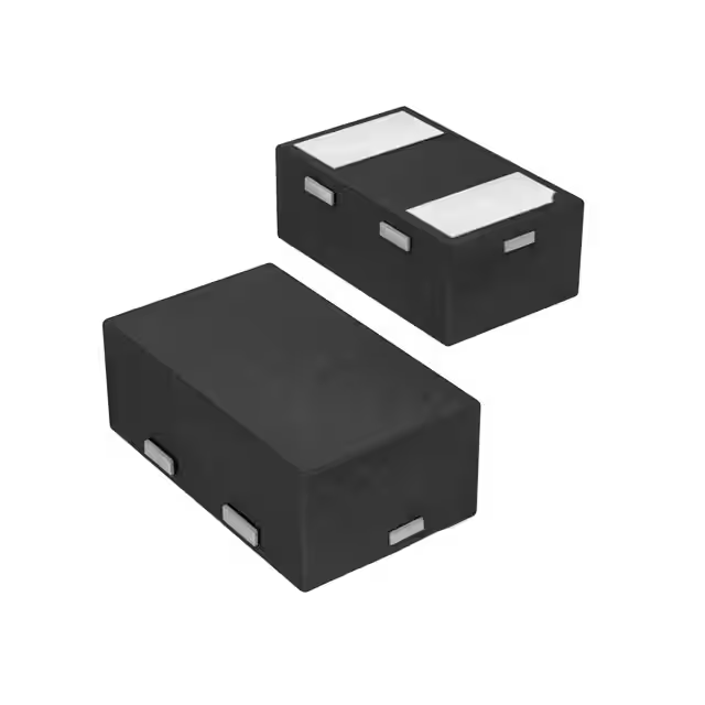
Alpha & Omega Semiconductor Inc. AOZ8211DI-03
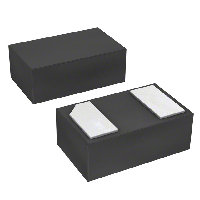
Part No.:
AOZ8211DI-03
Manufacturer:
Alpha & Omega Semiconductor Inc.
Category:
TVS Diodes
Package:
2-UDFN
Datasheet:
AetrixAOZ8211DI-03.pdf
Description:
TVS DIODE 3.3VWM 9.5VC 2DFN
Quantity:
Payment:
Payment
Shipping:
Shipping

Inventory:7,201

Please send an inquiry. Send us your inquiry, and we will respond immediately.

Part Number
Quantity*
Price
Name*
Company
Email*
Comments

Product details

Overview

AOZ8211DI-03 from Alpha and Omega Semiconductor is a unidirectional single-line TVS diode in a DFN 1.0 mm × 0.6 mm package, rated for 3.3 V working peak reverse voltage (VRWM), 5.5 A peak pulse current (IPP), and clamping voltage ≤7.5 V at 5 A. It delivers ±30 kV IEC 61000-4-2 contact/air ESD protection and operates across –40 °C to +85 °C ambient temperature, designed for high-speed data line protection in space-constrained portable electronics.

For engineers reviewing the AOZ8211DI-03 datasheet, pinout, applications, or equivalent options, key selection criteria include clamping voltage at specified IPP, VRWM alignment with signal rail voltage, low capacitance (11 pF), RoHS-compliant DFN footprint, and IEC/HBM ESD robustness for USB, keypad, and camera interface lines.

Technical Context

The AOZ8211DI-03 implements a silicon avalanche diode structure optimized for fast transient response (<1 ns rise time) and low clamping under 8/20 µs surge conditions. Its unidirectional configuration provides reverse-biased protection only, requiring correct anode-to-ground orientation on protected signal lines.

It operates with 0.75 V typical forward voltage at 10 mA and exhibits 11 pF junction capacitance at 0 V bias-critical for preserving signal integrity on high-speed interfaces up to 100 MHz. The device's 3.3 V VRWM targets 3.3 V logic rails while maintaining margin above typical IO voltage tolerances.

Key Specifications

ParameterValue and Actual Design Meaning
VRWM3.3 V - Matches standard 3.3 V I/O supply rails without false triggering during normal operation
VBR (min)3.7 V - Ensures reliable conduction onset above steady-state voltage, preventing leakage-induced noise
VCL @ IPP = 5 A≤7.5 V - Limits transient overvoltage to safe levels for downstream 3.3 V logic inputs
IPP (8/20 µs)5.5 A - Sustains industry-standard lightning/surge immunity per IEC 61000-4-5 Level 3
CJ @ 0 V, 1 MHz11 pF - Enables use on USB 2.0, SDIO, and I²C lines without signal degradation
ESD Rating (IEC 61000-4-2)±30 kV contact / ±30 kV air - Exceeds Level 4 requirement, supporting rugged handheld design
PackageDFN 1.0 mm × 0.6 mm × 0.5 mm - Enables placement adjacent to connectors or IC pads in ultra-thin devices

Pinout & Package

AOZ8211DI-03 uses a 2-terminal DFN package with exposed cathode pad for thermal and electrical grounding. The compact 1.0 mm × 0.6 mm outline supports high-density routing on thin PCBs.

Pin/TerminalCircuit RoleDesign Meaning
Anode (Pin 1)Signal line inputConnected directly to protected I/O trace; conducts transient current toward cathode when voltage exceeds VBR
Cathode (Pin 2)Ground return pathMust be tied to low-impedance system ground plane; serves as primary current sink during ESD events

Key Features

FeatureDesign Value
Ultra-low clamping voltage7.5 V max at 5 A enables compatibility with 3.3 V logic families including LVTTL and LVCMOS
Low junction capacitance11 pF minimizes insertion loss and timing skew on 480 Mbps USB 2.0 differential pairs
High ESD robustness±30 kV contact discharge withstand eliminates need for secondary board-level protection layers
Small-footprint DFN1.0 mm × 0.6 mm area reduces PCB real estate by >60% vs. SOD-323 alternatives
Low operating voltage rating3.3 V VRWM ensures no DC leakage or false triggering on nominal 3.3 V data lines

Applications

USB 2.0 Data LinesSmartphone Keypad Interfaces

Use Scenario: Protecting D+ and D– lines against ESD events during cable insertion or user handling.

IC Role / Device Role / Timing Role: Unidirectional TVS diode placed in series with each data line, grounded via short low-inductance trace.

Use Value: Maintains <11 pF loading to preserve eye diagram integrity while clamping transients to ≤7.5 V.

Use Scenario: Shielding mechanical keypad matrix rows/columns from user-finger ESD in consumer handsets.

IC Role / Device Role / Timing Role: Single-line TVS per key trace, oriented anode-to-signal, cathode-to-ground.

Use Value: Prevents latch-up or GPIO damage from ±30 kV contact discharges without adding series resistance.

Digital Camera Sensor InterfacesPortable GPS RF Front-End Control Lines

Use Scenario: Safeguarding MIPI CSI-2 clock and data lanes between image sensor and SoC.

IC Role / Device Role / Timing Role: Point-of-entry protection on each high-speed lane, placed within 3 mm of connector.

Use Value: 11 pF capacitance avoids jitter accumulation; 7.5 V clamping protects 3.3 V serializer inputs.

Use Scenario: Protecting SPI control lines (CS, SCLK, MOSI) connecting baseband processor to GPS module.

IC Role / Device Role / Timing Role: Discrete TVS per control signal, leveraging low VRWM to avoid interference with 3.3 V logic thresholds.

Use Value: Eliminates need for RC filters while meeting automotive-grade ESD immunity requirements.

Equivalent & Alternatives

The following parts are listed as comparable options for similar TVS diode applications.

Alternative PartTechnical DifferenceApplication DifferenceSelection Advice
SMAJ3.3ADO-214AC package (4.5 mm × 2.7 mm); 600 W peak power; 12.3 V clamping @ 5.9 A; 350 pF capacitanceNot suitable for high-speed data lines due to high capacitance; intended for power rail or low-frequency signal protectionSelect SMAJ3.3A only for non-high-speed, space-tolerant designs where low capacitance is not required
TPD2E001DRYR2-channel unidirectional TVS in DFN 1.0 mm × 0.6 mm; 3.3 V VRWM; 12 pF per channel; ±8 kV IEC 61000-4-2 contactLower ESD rating limits use in premium consumer devices; dual-channel integration reduces component count but increases cost per lineChoose TPD2E001DRYR when protecting two adjacent lines with shared layout constraints and lower ESD requirements apply

Compared with SMAJ3.3A and TPD2E001DRYR, the AOZ8211DI-03 uniquely balances ultra-small size, ±30 kV ESD robustness, and 11 pF capacitance-making it optimal for single-line, high-speed, space-critical protection where both signal fidelity and ruggedness are mandatory.

Availability

AOZ8211DI-03 is available at Aetrix Electronics and suitable for smartphone front-panel interfaces, USB-C accessory detection circuits, and portable medical monitor sensor links requiring stable component supply, consistent RoHS compliance, and guaranteed lifecycle continuity.

Supply support for AOZ8211DI-03 includes scheduled delivery planning, volume procurement assistance, BOM continuity management, traceable sourcing, and lifecycle availability coordination for OEM customers, industrial embedded developers, connected-device designers, and electronics production programs.

Manufacturer

Alpha and Omega Semiconductor (AOS) is a fabless power semiconductor company specializing in MOSFETs, TVS diodes, and power ICs for efficiency-critical applications.

The AOZ8211DI family was developed to address miniaturization and ESD resilience demands in mobile and wearable electronics, delivering high-performance transient suppression in sub-1 mm² footprints.

FAQ

What is the maximum clamping voltage of the AOZ8211DI-03 at 5 A peak pulse current?

The AOZ8211DI-03 has a maximum clamping voltage (VCL) of 7.5 V at 5 A peak pulse current under 8/20 µs waveform conditions. This value is specified in the Electrical Characteristics table on page 3 of the Rev. 5.0 datasheet and ensures safe voltage limiting for 3.3 V logic interfaces during surge events. The AOZ8211DI-03 maintains this performance across its full operating temperature range.

Is the AOZ8211DI-03 unidirectional or bidirectional, and how does that affect circuit placement?

The AOZ8211DI-03 is a unidirectional TVS diode, configured with anode and cathode terminals. It must be placed with the anode connected to the protected signal line and the cathode tied to ground-providing protection only against negative transients relative to ground. This polarity-sensitive layout is confirmed in the "Typical Application" diagram on page 2 of the AOZ8211DI datasheet. Incorrect orientation renders the AOZ8211DI-03 ineffective.

What is the junction capacitance of the AOZ8211DI-03, and why does it matter for high-speed interfaces?

The AOZ8211DI-03 exhibits 11 pF typical junction capacitance at 0 V bias and 1 MHz, as measured per the Electrical Characteristics table. This low value prevents signal distortion, timing skew, and attenuation on high-speed lines such as USB 2.0, MIPI CSI-2, and SDIO. Higher capacitance would degrade eye diagrams and increase bit error rates-making the AOZ8211DI-03 suitable where signal integrity is critical.

Does the AOZ8211DI-03 meet IEC 61000-4-2 Level 4, and what ESD levels does it actually exceed?

Yes, the AOZ8211DI-03 exceeds IEC 61000-4-2 Level 4 requirements: it is rated for ±30 kV air discharge and ±30 kV contact discharge, versus Level 4's minimum of ±15 kV air and ±8 kV contact. This performance is documented in the Features section (page 1) and Absolute Maximum Ratings table (page 2) of the AOZ8211DI Rev. 5.0 datasheet. The AOZ8211DI-03 thus supports premium-grade ESD hardening in consumer and industrial handhelds.

What is the operating temperature range of the AOZ8211DI-03, and is it suitable for automotive cabin applications?

AOZ8211DI-03 is rated for an ambient operating temperature range of –40 °C to +85 °C, as stated in the Maximum Operating Ratings table. While this covers many industrial and consumer environments, it does not meet extended automotive temperature requirements (–40 °C to +105 °C or +125 °C) defined in AEC-Q200. Therefore, AOZ8211DI-03 is appropriate for infotainment front-panel interfaces or portable diagnostic tools-but not under-hood or instrument cluster applications.

AOZ8211DI-03 Specifications

Product attributes
Attribute value
Manufacturer:
Alpha & Omega Semiconductor Inc.
Package/Case:
2-UDFN
Series:
-
Packaging:
Tape & Reel (TR)
Product Status:
Active
Type:
Zener
Unidirectional Channels:
1
Bidirectional Channels:
-
Voltage - Reverse Standoff (Typ):
3.3V (Max)
Voltage - Breakdown (Min):
3.7V
Voltage - Clamping (Max) @ Ipp:
9.5V
Current - Peak Pulse (10/1000µs):
6A (8/20µs)
Power - Peak Pulse:
55W
Power Line Protection:
No
Applications:
General Purpose
Capacitance @ Frequency:
11pF @ 1MHz
Operating Temperature:
-40°C ~ 85°C (TJ)
Grade:
-
Qualification:
-
Mounting Type:
Surface Mount
Supplier Device Package:
2-DFN (1x0.6)

AOZ8211DI-03 FAQ

1.How can I place an order for AOZ8211DI-03 through Aetrix?

Please submit a Request for Quotation (RFQ) for AOZ8211DI-03 on Aetrix. Our sales agent will provide a competitive quotation and guide you through the order confirmation once you accept the terms.

2.Are the price and stock information for AOZ8211DI-03 reliable?

The price and inventory of AOZ8211DI-03 are updated periodically and may fluctuate due to market conditions. Stock and pricing data are typically refreshed every 24 hours. Quotation validity for AOZ8211DI-03 is usually 5 days.

3.What payment methods are accepted for AOZ8211DI-03?

We accept Wire Transfer, PayPal, Credit Card, Western Union, MoneyGram, and Escrow for AOZ8211DI-03 transactions.

Note: Certain payment methods may incur a processing fee.

4.How is shipping managed for AOZ8211DI-03?

AOZ8211DI-03 orders can be shipped via leading logistics carriers, including DHL, UPS, FedEx, TNT, or Registered Mail.

Once your AOZ8211DI-03 order is processed, you will receive an email with the shipment details and tracking number.

Note: Tracking information may take up to 24 hours to appear. Express delivery typically takes 3–5 business days.

5.How can I obtain technical support or documentation for AOZ8211DI-03?

For technical support, including AOZ8211DI-03 datasheets, pinout diagrams, or application guidance, please contact our engineering support team. They can provide detailed documentation and assistance for your AOZ8211DI-03 requirements.

6.How does Aetrix verify that AOZ8211DI-03 is sourced from the original manufacturer or authorized distributors?

All AOZ8211DI-03 products on Aetrix are procured from qualified distributors and authorized channels. Our dedicated quality assurance team conducts strict verification, including traceability checks and, if necessary, third-party testing. This ensures that AOZ8211DI-03 meets industry standards.

7.What is the process for return or replacement of AOZ8211DI-03?

All AOZ8211DI-03 units undergo pre-shipment inspection (PSI). If there is an issue with AOZ8211DI-03, returns or replacements are accepted under the following conditions:

1.Quantity discrepancies, incorrect items, or visible external defects (such as breakage or corrosion), acknowledged by Aetrix.

2.The issue is reported within 90 days of delivery.

3.The AOZ8211DI-03 part is unused and in its original packaging.

Return procedure for AOZ8211DI-03:

1.Submit a request within 90 days.

2.Obtain a Return Material Authorization (RMA) from Aetrix.

AOZ8211DI-03 Tags
  • AOZ8211DI-03
  • AOZ8211DI-03 PDF
  • AOZ8211DI-03 Datasheet
  • AOZ8211DI-03 Specifications
  • AOZ8211DI-03 Images
  • Alpha & Omega Semiconductor Inc.
  • Alpha & Omega Semiconductor Inc. AOZ8211DI-03
  • Buy AOZ8211DI-03
  • AOZ8211DI-03 Price
  • AOZ8211DI-03 Distributor
  • AOZ8211DI-03 Supplier
  • AOZ8211DI-03 Wholesale
Related Products
ESD9B5.0ST5G
ESD9B5.0ST5G

onsemi

DESD3V3E1BL-7B
DESD3V3E1BL-7B

Diodes Incorporated

ESD5Z3.3T1G
ESD5Z3.3T1G

onsemi

D5V0H1B2LP-7B
D5V0H1B2LP-7B

Diodes Incorporated

D5V0P1B2LP-7B
D5V0P1B2LP-7B

Diodes Incorporated

DESD5V0U1BA-7
DESD5V0U1BA-7

Diodes Incorporated

ESD5Z5.0T1G
ESD5Z5.0T1G

onsemi

DESD5V0U1BB-7
DESD5V0U1BB-7

Diodes Incorporated

D12V0L1B2LP-7B
D12V0L1B2LP-7B

Diodes Incorporated

PESD2V0Y1BSFYL
PESD2V0Y1BSFYL

Nexperia USA Inc.

DF2S5M4CT,L3F
DF2S5M4CT,L3F

Toshiba Semiconductor and Storage

D5V0L1B2WS-7
D5V0L1B2WS-7

Diodes Incorporated

Tech Hub

Search

Search

PRODUCT

PRODUCT

PHONE

PHONE

USER

USER