
 My Inquiry
 My Account


Diodes Incorporated D5V0L1B2S9-7
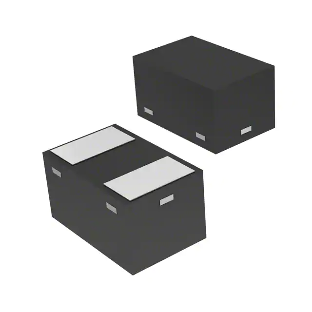
- Part No.:
- D5V0L1B2S9-7
- Manufacturer:
- Diodes Incorporated
- Category:
- TVS Diodes
- Package:
- SOD-923
- Datasheet:
-
 D5V0L1B2S9-7.pdf
- Description:
- TVS DIODE 5VWM 14VC SOD923
- Quantity:
- Payment:

- Shipping:

Inventory:759,064
Please send an inquiry. Send us your inquiry, and we will respond immediately.
Product details
Overview
D5V0L1B2S9-7 from Diodes Incorporated is a bidirectional transient voltage suppression (TVS) diode designed for ESD protection of high-speed data lines in portable electronics. It features 5 V reverse standoff voltage, ±30 kV IEC 61000-4-2 contact/air ESD immunity, 15 pF typical input capacitance, 6 A peak pulse current, and SOD923 package - enabling robust protection in space-constrained interfaces like USB 2.0 and audio jacks.
For engineers reviewing the D5V0L1B2S9-7 datasheet, D5V0L1B2S9-7 pinout, D5V0L1B2S9-7 application, or D5V0L1B2S9-7 equivalent, key selection criteria include low clamping voltage under 6 A surge, sub-20 pF channel capacitance for signal integrity, bidirectional polarity, RoHS-compliant lead-free construction, and compatibility with automated SMT assembly on FR-4 PCBs.
Technical Context
This TVS diode operates as a voltage-clamped shunt protector across differential or single-ended signal paths. Its silicon avalanche structure triggers at 6 V breakdown (VBR), clamps transients to ≤14.0 V at 6 A (8/20 µs), and maintains leakage <100 nA at 5 V - ensuring minimal loading on sensitive I/O pins.
The device uses a monolithic dual-anode/dual-cathode configuration in SOD923 to achieve true bidirectional behavior without external biasing. Its 15 pF input capacitance (measured at 0 V, 1 MHz) and low differential resistance (<0.2 Ω at 1 A) preserve signal edge fidelity in high-frequency applications up to ~500 MHz.
Key Specifications
| Parameter | Value and Actual Design Meaning |
|---|---|
| Reverse Standoff Voltage | 5 V - Maximum continuous operating voltage before conduction begins; sets upper limit for protected line voltage. |
| Breakdown Voltage (VBR) | 6 V min @ 1 mA - Threshold where avalanche conduction initiates reliably during ESD events. |
| Clamping Voltage (VCL) | 11.5–14.0 V @ 6 A, 8/20 µs - Peak voltage seen by downstream circuitry during worst-case surge. |
| Input Capacitance (CIN) | 15 pF typ @ 0 V, 1 MHz - Low enough to avoid signal distortion on USB 2.0, HDMI, or audio lines. |
| ESD Rating | ±30 kV contact & air per IEC 61000-4-2 - Meets highest industrial ESD immunity class without external filtering. |
| Peak Pulse Power | 84 W @ 8/20 µs - Sustains multi-kV ESD pulses without degradation in compact SOD923 footprint. |
| Leakage Current | 10–100 nA @ 5 V - Negligible DC loading on battery-powered sensor or interface circuits. |
Pinout & Package
Package: SOD923 - ultra-small surface-mount plastic case (0.90 × 0.40 × 0.60 mm), UL 94V-0 rated, moisture sensitivity level 1, matte tin-plated alloy 42 leadframe.
| Pin/Terminal | Circuit Role | Design Meaning |
|---|---|---|
| Pin 1 | Anode 1 / Cathode 2 | Bidirectional terminal - forms one side of symmetrical clamping path between I/O and ground. |
| Pin 2 | Cathode 1 / Anode 2 | Bidirectional terminal - completes symmetrical clamping path; no polarity marking required. |
Key Features
| Feature | Design Value |
|---|---|
| IEC 61000-4-2 ESD Protection | ±30 kV contact & air - eliminates need for secondary ESD filters in handheld UI designs. |
| Low Input Capacitance | 15 pF typ - preserves rise time and eye diagram integrity on 480 Mbps USB 2.0 signals. |
| Bidirectional Clamping | Symmetrical VBR = 6 V - protects AC-coupled or floating lines (e.g., headphone jack, HDMI DDC) without bias network. |
| Lead-Free & Green Construction | Halogen- and antimony-free, <900 ppm Br/Cl, <1000 ppm Sb - meets strict environmental compliance for global consumer shipments. |
Applications
| USB 2.0 Data Lines | Smartphone Audio Jacks |
|---|---|
Use Scenario: Protecting D+ and D− pins of USB 2.0 transceivers against repeated plug/unplug ESD events. IC Role / Device Role: Bidirectional shunt TVS placed directly at connector, clamping transients before they reach PHY IC. Use Value: 15 pF capacitance avoids signal integrity loss at 480 Mbps; ±30 kV rating exceeds USB-IF ESD test requirements. | Use Scenario: Safeguarding 3.5 mm TRRS audio jack contacts (mic, left/right, ground) in smartphones against user-hand ESD. IC Role / Device Role: Single-channel bidirectional TVS mounted adjacent to jack, routing ESD current to chassis ground. Use Value: Sub-1 mm² SOD923 footprint fits tight board space near jack; low leakage prevents DC offset in analog mic path. |
| Digital Camera Interface | Portable Medical Sensors |
Use Scenario: Shielding MIPI CSI-2 data lanes between image sensor and processor from handling ESD during module assembly. IC Role / Device Role: Per-lane TVS on high-speed differential pairs, minimizing inter-pair skew via matched capacitance. Use Value: 15 pF typ ensures <0.1 dB insertion loss at 500 MHz; 6 V VRWM aligns with 3.3 V I/O supply rails. | Use Scenario: Protecting analog front-end inputs of wearable ECG or SpO₂ sensors exposed to clinical environment ESD. IC Role / Device Role: Low-leakage (10 nA typ) TVS on sensor signal path, preventing false triggers or ADC saturation. Use Value: 100 nA max IR at 5 V avoids baseline drift in µV-level bio-potential measurements. |
Equivalent & Alternatives
The following parts are listed as comparable options for similar ESD protection applications.
| Alternative Part | Technical Difference | Application Difference | Selection Advice |
|---|---|---|---|
| SP1001-01UTG | Unidirectional; 5.5 V VRWM; 12 pF CIN; 4 A IPP | Requires correct polarity placement; lower capacitance but reduced surge rating. | Prefer when signal path is DC-biased and layout allows polarity-aware placement. |
| ESD5Z5.0T1G | Bidirectional; 5.0 V VRWM; 25 pF CIN; 6 A IPP | Higher capacitance limits use to <100 Mbps interfaces; same SOD-523 package size. | Acceptable for low-speed UART or I²C where 25 pF does not degrade timing margins. |
Compared with SP1001-01UTG and ESD5Z5.0T1G, D5V0L1B2S9-7 uniquely balances bidirectional operation, 6 A surge capability, and 15 pF capacitance in SOD923 - making it optimal for high-speed, polarity-agnostic protection where board space and signal fidelity are jointly constrained.
Availability
D5V0L1B2S9-7 is available at Aetrix Electronics and suitable for cellular handsets, portable medical sensors, and USB 2.0 peripheral designs requiring stable component supply across high-mix, low-volume production runs.
Supply support for D5V0L1B2S9-7 includes scheduled delivery planning, volume procurement assistance, BOM continuity management, traceable sourcing, and lifecycle availability coordination for OEM customers, industrial embedded developers, connected-device designers, and electronics production programs.
Manufacturer
Diodes Incorporated is a global manufacturer of discrete semiconductors and analog ICs, headquartered in Plano, Texas, with design and manufacturing operations across Asia and the Americas.
This device belongs to Diodes' ESD protection product line, engineered specifically for ultra-low-capacitance, high-surge immunity in miniaturized portable electronics - emphasizing board-space efficiency and compliance with IEC 61000-4-2 Level 4.
FAQ
What is the maximum clamping voltage of D5V0L1B2S9-7 at 6 A surge current?
The clamping voltage is specified as 11.5 V (typical) to 14.0 V (maximum) at 6 A, 8/20 µs waveform. This value represents the peak voltage imposed on the protected line during worst-case ESD transients, ensuring downstream ICs with 13.2 V absolute maximum ratings remain within safe operating limits.
Can D5V0L1B2S9-7 be used on a 3.3 V I/O line?
Yes - its 5 V reverse standoff voltage (VRWM) provides sufficient margin above 3.3 V nominal operation, while leakage remains below 100 nA at that bias. The 6 V minimum breakdown ensures reliable triggering only during ESD events, avoiding false conduction during normal signal swings.
Is the SOD923 package compatible with standard reflow profiles?
Yes - the SOD923 package has moisture sensitivity level 1 and is qualified for IPC/JEDEC J-STD-020 standard reflow. Its matte tin finish and alloy 42 leadframe ensure reliable solderability using SnPb or lead-free SAC305 profiles, with peak temperatures up to 260 °C.
Does D5V0L1B2S9-7 require external series impedance for optimal ESD performance?
No - it is designed for direct placement across the protected line and ground, with no series resistor needed. Its low dynamic resistance (<0.2 Ω) and fast response (<1 ns) enable effective clamping without added components, though board layout (short traces, solid ground plane) remains critical for achieving full ±30 kV rating.
D5V0L1B2S9-7 Specifications
- Product attributes
- Attribute value
- Manufacturer:
- Diodes Incorporated
- Package/Case:
- SOD-923
- Series:
- -
- Packaging:
- Tape & Reel (TR)
- Product Status:
- Active
- Type:
- Zener
- Unidirectional Channels:
- -
- Bidirectional Channels:
- 1
- Voltage - Reverse Standoff (Typ):
- 5V (Max)
- Voltage - Breakdown (Min):
- 6V
- Voltage - Clamping (Max) @ Ipp:
- 14V
- Current - Peak Pulse (10/1000µs):
- 6A (8/20µs)
- Power - Peak Pulse:
- 84W
- Power Line Protection:
- No
- Applications:
- General Purpose
- Capacitance @ Frequency:
- 15pF @ 1MHz
- Operating Temperature:
- -65°C ~ 150°C (TJ)
- Grade:
- -
- Qualification:
- -
- Mounting Type:
- Surface Mount
- Supplier Device Package:
- SOD-923
D5V0L1B2S9-7 FAQ
1.How can I place an order for D5V0L1B2S9-7 through Aetrix?
Please submit a Request for Quotation (RFQ) for D5V0L1B2S9-7 on Aetrix. Our sales agent will provide a competitive quotation and guide you through the order confirmation once you accept the terms.
2.Are the price and stock information for D5V0L1B2S9-7 reliable?
The price and inventory of D5V0L1B2S9-7 are updated periodically and may fluctuate due to market conditions. Stock and pricing data are typically refreshed every 24 hours. Quotation validity for D5V0L1B2S9-7 is usually 5 days.
3.What payment methods are accepted for D5V0L1B2S9-7?
We accept Wire Transfer, PayPal, Credit Card, Western Union, MoneyGram, and Escrow for D5V0L1B2S9-7 transactions.
Note: Certain payment methods may incur a processing fee.
4.How is shipping managed for D5V0L1B2S9-7?
D5V0L1B2S9-7 orders can be shipped via leading logistics carriers, including DHL, UPS, FedEx, TNT, or Registered Mail.
Once your D5V0L1B2S9-7 order is processed, you will receive an email with the shipment details and tracking number.
Note: Tracking information may take up to 24 hours to appear. Express delivery typically takes 3–5 business days.
5.How can I obtain technical support or documentation for D5V0L1B2S9-7?
For technical support, including D5V0L1B2S9-7 datasheets, pinout diagrams, or application guidance, please contact our engineering support team. They can provide detailed documentation and assistance for your D5V0L1B2S9-7 requirements.
6.How does Aetrix verify that D5V0L1B2S9-7 is sourced from the original manufacturer or authorized distributors?
All D5V0L1B2S9-7 products on Aetrix are procured from qualified distributors and authorized channels. Our dedicated quality assurance team conducts strict verification, including traceability checks and, if necessary, third-party testing. This ensures that D5V0L1B2S9-7 meets industry standards.
7.What is the process for return or replacement of D5V0L1B2S9-7?
All D5V0L1B2S9-7 units undergo pre-shipment inspection (PSI). If there is an issue with D5V0L1B2S9-7, returns or replacements are accepted under the following conditions:
1.Quantity discrepancies, incorrect items, or visible external defects (such as breakage or corrosion), acknowledged by Aetrix.
2.The issue is reported within 90 days of delivery.
3.The D5V0L1B2S9-7 part is unused and in its original packaging.
Return procedure for D5V0L1B2S9-7:
1.Submit a request within 90 days.
2.Obtain a Return Material Authorization (RMA) from Aetrix.
D5V0L1B2S9-7 Tags
-
ESD9B5.0ST5G
onsemi
-
DESD3V3E1BL-7B
Diodes Incorporated
-
ESD5Z3.3T1G
onsemi
-
D5V0H1B2LP-7B
Diodes Incorporated
-
D5V0P1B2LP-7B
Diodes Incorporated
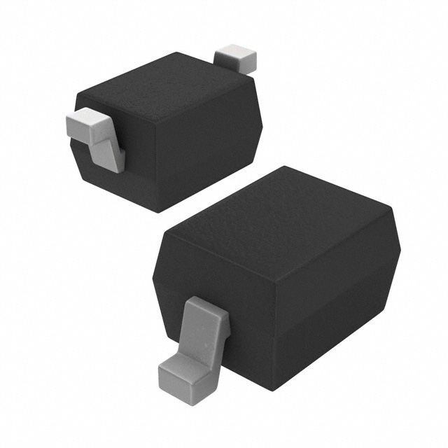
-
DESD5V0U1BA-7
Diodes Incorporated
-
ESD5Z5.0T1G
onsemi
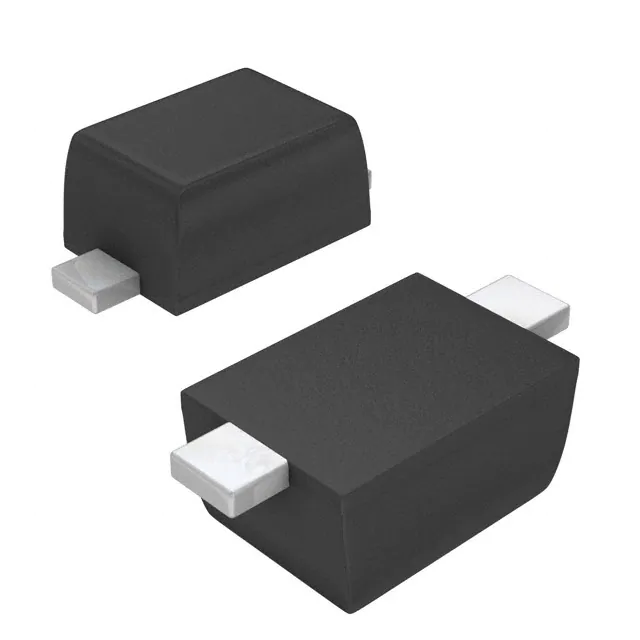
-
DESD5V0U1BB-7
Diodes Incorporated
-
D12V0L1B2LP-7B
Diodes Incorporated
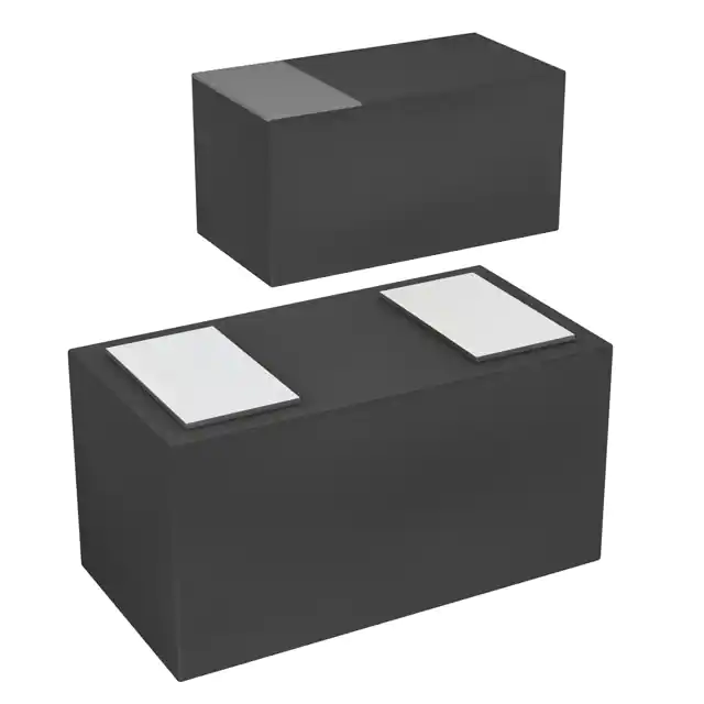
-
PESD2V0Y1BSFYL
Nexperia USA Inc.
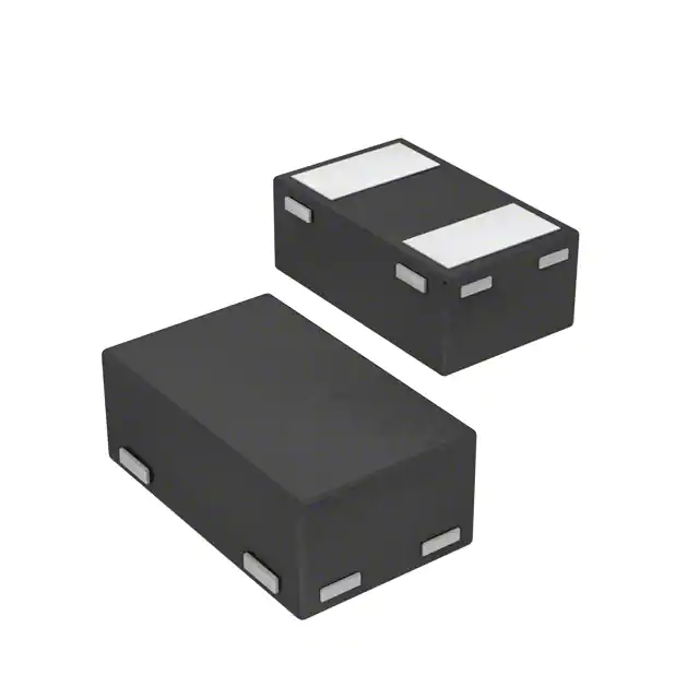
-
DF2S5M4CT,L3F
Toshiba Semiconductor and Storage
-
D5V0L1B2WS-7
Diodes Incorporated
Tech Hub

Jumper cables guide covering safe connection order, red and black clamp placement, final ground connection, cable gauge, length, clamp quality, copper vs CCA cables, jump starter comparison and battery…

LDO regulator guide covering low dropout voltage, power dissipation, thermal design, PSRR, output noise, capacitor stability, adjustable LDO circuits, LDO vs buck converter and datasheet selection chec…

Conditional Access Module guide covering CAM meaning, CI/CI+ interface, smart card authorization, DVB security workflow, TV and set-top box compatibility, internal electronics, ESD protection, connecto…

Guide to electronic component obsolescence covering EOL risk, PCN/PDN notices, last-time buy planning, replacement options, form-fit-function validation, counterfeit risk and BOM lifecycle management.

18650 battery guide covering lithium-ion cell basics, 3.6V/3.7V voltage, 4.2V charging, mAh and Wh capacity, protected cells, chargers, BMS, series-parallel packs, holders, welding and sourcing checks.…

Hall effect sensor guide covering working principle, linear and digital sensors, Arduino circuits, current sensing, speed detection, automotive applications, A3144 examples, signal filtering and datash…

Product Change Notification guide for electronic components, covering PCN meaning, PCN vs PDN/EOL, common change types, risk levels, form-fit-function review, engineering validation, BOM control, LTB/L…

A practical guide to blend door actuators, covering HVAC function, symptoms, location, AC and heater issues, reset and calibration, replacement cost, electrical diagnosis, compatibility checks, and rep…

Engineering guide to Raspberry Pi alternatives, covering chip-level differences, Orange Pi, ROCK, Jetson, Banana Pi, NanoPi, Compute Module, Pico, GPIO, camera, HAT compatibility, and replacement risks…

Engineering guide to dynamic load response testing for high-current buck converters, covering load step setup, slew rate, Vcore undershoot, overshoot, recovery time, probe location, output capacitors a…


