
 My Inquiry
 My Account


Toshiba Semiconductor and Storage DF3D29FU,LF
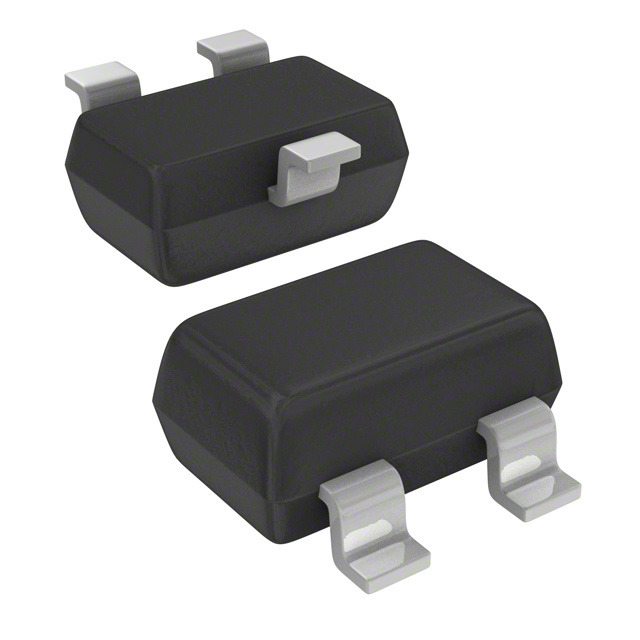
- Part No.:
- DF3D29FU,LF
- Manufacturer:
- Toshiba Semiconductor and Storage
- Category:
- TVS Diodes
- Package:
- SC-70, SOT-323
- Datasheet:
-
 DF3D29FU,LF.pdf
- Description:
- TVS DIODE 24VWM 47VC USM
- Quantity:
- Payment:

- Shipping:

Inventory:7,527
Please send an inquiry. Send us your inquiry, and we will respond immediately.
Product details
Overview
DF3D29FU,LF from Toshiba Electronic Devices & Storage Corporation is an AEC-Q101-qualified ESD protection diode in USM package, featuring ±25 kV IEC61000-4-2 contact ESD immunity, 24 V working peak reverse voltage, and 47 V max clamp voltage at 3 A peak pulse current. It serves as a unidirectional transient voltage suppressor for high-speed data lines in automotive infotainment interfaces.
For engineers reviewing the DF3D29FU,LF datasheet, DF3D29FU,LF pinout, DF3D29FU,LF application, or DF3D29FU,LF equivalent, key selection criteria include IEC61000-4-2/ISO10605 ESD rating compliance, low dynamic resistance (≤10 Ω), sub-1 pF typical capacitance, and AEC-Q101 qualification for automotive signal line protection.
Technical Context
This device implements a silicon epitaxial planar unidirectional TVS structure optimized for fast response to electrostatic discharge events. Its clamping behavior is characterized under IEC61000-4-5 8/20 µs pulses with guaranteed VC ≤ 47 V at IPP = 3 A and dynamic resistance ≤ 10 Ω.
The DF3D29FU,LF operates with VRWM = 24 V and VBR ≥ 26 V (min), ensuring reliable blocking during normal signal operation while triggering within 1 ns to limit transient overvoltage. Total capacitance is specified at 9–10 pF (typ/max) at 0 V, supporting USB 2.0 and HDMI 1.4 signal integrity requirements.
Key Specifications
| Parameter | Value and Actual Design Meaning |
|---|---|
| ESD Rating (IEC61000-4-2 Contact) | ±25 kV - meets automotive-level ESD immunity for exposed connectors |
| Working Peak Reverse Voltage | 24 V - supports 24 V nominal supply rail protection without leakage |
| Clamp Voltage @ 3 A | 47 V max - limits downstream IC stress during 8/20 µs transients |
| Dynamic Resistance | 10 Ω max - ensures rapid voltage collapse and low let-through energy |
| Total Capacitance | 10 pF max @ 0 V, 1 MHz - preserves signal integrity on 480 Mbps USB 2.0 lines |
| Reverse Leakage Current | 0.1 µA max @ 24 V - minimizes standby power loss in always-on interfaces |
| AEC-Q101 Qualified | Yes - validated for automotive temperature cycling, HTRB, and ESD stress per Rev.6.0.A |
Pinout & Package
DF3D29FU,LF uses the USM (Ultra Small Mold) package: 1.2 × 0.8 × 0.38 mm, 3-terminal surface-mount, weight 6.0 mg (typ). Pin 1 and Pin 2 are anode and cathode terminals; Pin 3 is GND.
| Pin/Terminal | Circuit Role | Design Meaning |
|---|---|---|
| Pin 1 | Anode | Input terminal for protected signal line; connects to I/O trace before ESD event |
| Pin 2 | Cathode | Output terminal tied to protected IC input; sinks transient current to GND |
| Pin 3 | GND | Low-inductance return path to system ground plane; critical for effective clamping |
Key Features
| Feature | Design Value |
|---|---|
| Automotive-grade qualification | AEC-Q101 qualified - enables use in automotive infotainment, ADAS camera links, and body control modules |
| Low clamping voltage | VC ≤ 47 V @ 3 A - protects 3.3 V/5 V logic inputs against ISO10605-induced overshoot |
| Ultra-low capacitance | Ct = 9–10 pF - maintains <0.1 dB insertion loss at 240 MHz for USB 2.0 eye diagram compliance |
| Fast response time | <1 ns turn-on - triggers before sensitive CMOS gate oxide breakdown during ESD strike |
| Robust thermal performance | Tj = -55 to +150 °C - sustains operation in engine bay and dashboard environments |
Applications
| USB 2.0 Interface Protection | HDMI 1.4 Hot-Plug Detection Line |
|---|---|
Use Scenario: Protecting D+ and D− differential pairs in automotive head-unit USB ports from connector mating ESD. IC Role / Device Role / Timing Role: Unidirectional TVS diode placed between connector and USB transceiver IC. Use Value: Prevents latch-up and gate oxide damage in USB PHY with <10 pF loading and ±25 kV contact immunity. | Use Scenario: Safeguarding HDMI HPD (Hot-Plug Detect) signal line in vehicle display systems during cable insertion/removal. IC Role / Device Role / Timing Role: Clamp diode connected between HPD pin and chassis ground to shunt ESD energy. Use Value: Ensures reliable plug detection without false interrupts or permanent HPD pin failure under ±30 kV air discharge. |
| Automotive Camera Serial Link (GMSL) | Touchscreen Controller Data Lines |
Use Scenario: ESD protection on bidirectional GMSL serial link pins in rear-view camera modules exposed to trunk environment. IC Role / Device Role / Timing Role: Low-capacitance TVS on each data lane upstream of serializer IC. Use Value: Maintains 3 Gbps signal fidelity while suppressing >140 W peak pulse energy per IEC61000-4-5. | Use Scenario: Shielding I²C SDA/SCL lines connecting capacitive touchscreen controller to MCU in center console displays. IC Role / Device Role / Timing Role: Dual-line ESD suppressor with matched capacitance on both signals. Use Value: Eliminates touch ghosting and reset events caused by finger-contact ESD on glass surface. |
Equivalent & Alternatives
The following parts are listed as comparable options for similar ESD protection applications.
| Alternative Part | Technical Difference | Application Difference | Selection Advice |
|---|---|---|---|
| TPD2E001DRYR | Lower VRWM (5.5 V), higher capacitance (11 pF typ), same USON-6 package footprint but different pinout | Targeted for 3.3 V logic; not rated for 24 V systems or AEC-Q101 | Select when protecting low-voltage digital I/O with tighter board space constraints |
| ESD5Z3.3T5G | Same VRWM (3.3 V), lower ESD rating (±12 kV contact), SOD-523 package (1.6 × 0.8 mm) | Cost-optimized for consumer electronics; lacks automotive qualification and high-energy clamping | Choose for non-automotive applications where IEC61000-4-2 ±8 kV suffices |
Compared with TPD2E001DRYR and ESD5Z3.3T5G, the DF3D29FU,LF delivers higher working voltage margin, superior automotive qualification, and lower dynamic resistance-making it the only option among the three validated for 24 V automotive signal line protection with ±25 kV ESD immunity.
Availability
DF3D29FU,LF is available at Aetrix Electronics and suitable for automotive infotainment, ADAS camera interfaces, and industrial HMI touchscreens requiring stable component supply across extended temperature ranges and long production lifecycles.
Supply support for DF3D29FU,LF includes scheduled delivery planning, volume procurement assistance, BOM continuity management, traceable sourcing, and lifecycle availability coordination for OEM customers, industrial embedded developers, connected-device designers, and electronics production programs.
Manufacturer
Toshiba Electronic Devices & Storage Corporation designs and manufactures discrete semiconductors, power devices, and logic ICs with emphasis on automotive, industrial, and consumer reliability standards.
The DF3D29FU,LF belongs to Toshiba's AEC-Q101-qualified ESD protection diode product line, engineered specifically for robust transient suppression on high-speed automotive data buses including USB, HDMI, and GMSL.
FAQ
What is the maximum working voltage supported by DF3D29FU,LF?
The DF3D29FU,LF has a working peak reverse voltage (VRWM) of 24 V, meaning it reliably blocks voltages up to 24 V in normal operation without significant leakage. This makes DF3D29FU,LF suitable for protecting 24 V automotive signal lines such as CAN FD stubs or LIN bus interfaces where transient suppression is required without DC conduction.
Is DF3D29FU,LF qualified for automotive applications?
Yes, DF3D29FU,LF is AEC-Q101 qualified per Rev.6.0.A documentation, having passed stress tests including temperature cycling, high-temperature reverse bias, and ESD robustness per IEC61000-4-2 and ISO10605. This qualification confirms DF3D29FU,LF for use in automotive infotainment, body electronics, and ADAS subsystems where reliability under harsh environmental conditions is mandatory.
What is the clamping voltage of DF3D29FU,LF at 3 A peak pulse current?
The DF3D29FU,LF exhibits a maximum clamp voltage (VC) of 47 V when subjected to a 3 A peak pulse current per IEC61000-4-5 8/20 µs waveform. This value is measured under standardized test conditions and ensures that downstream ICs-such as USB transceivers or HDMI receivers-are exposed to no more than 47 V during surge events, well below typical absolute maximum ratings.
Does DF3D29FU,LF have low capacitance suitable for high-speed data lines?
Yes, DF3D29FU,LF specifies total capacitance (Ct) of 9–10 pF at 0 V and 1 MHz, enabling use on USB 2.0 (480 Mbps), HDMI 1.4 (up to 3.4 Gbps), and other high-speed interfaces without degrading signal rise/fall times or eye opening. The low capacitance is achieved via optimized junction design and USM package parasitics, making DF3D29FU,LF appropriate for precision analog and digital signal paths.
What package type does DF3D29FU,LF use and how many terminals does it have?
DF3D29FU,LF uses the USM (Ultra Small Mold) package measuring 1.2 × 0.8 × 0.38 mm with three terminals: Pin 1 (anode), Pin 2 (cathode), and Pin 3 (GND). This compact 3-pin configuration allows placement directly at connector entry points with minimal PCB area, and its low profile supports automated optical inspection and reflow soldering in high-density automotive PCB assemblies.
DF3D29FU,LF Specifications
- Product attributes
- Attribute value
- Manufacturer:
- Toshiba Semiconductor and Storage
- Package/Case:
- SC-70, SOT-323
- Series:
- -
- Packaging:
- Tape & Reel (TR)
- Product Status:
- Active
- Type:
- Zener
- Unidirectional Channels:
- 2
- Bidirectional Channels:
- -
- Voltage - Reverse Standoff (Typ):
- 24V
- Voltage - Breakdown (Min):
- 26V
- Voltage - Clamping (Max) @ Ipp:
- 47V
- Current - Peak Pulse (10/1000µs):
- 3A (8/20µs)
- Power - Peak Pulse:
- 140W
- Power Line Protection:
- No
- Applications:
- -
- Capacitance @ Frequency:
- 9pF @ 1MHz
- Operating Temperature:
- -
- Grade:
- -
- Qualification:
- -
- Mounting Type:
- Surface Mount
- Supplier Device Package:
- USM
DF3D29FU,LF FAQ
1.How can I place an order for DF3D29FU,LF through Aetrix?
Please submit a Request for Quotation (RFQ) for DF3D29FU,LF on Aetrix. Our sales agent will provide a competitive quotation and guide you through the order confirmation once you accept the terms.
2.Are the price and stock information for DF3D29FU,LF reliable?
The price and inventory of DF3D29FU,LF are updated periodically and may fluctuate due to market conditions. Stock and pricing data are typically refreshed every 24 hours. Quotation validity for DF3D29FU,LF is usually 5 days.
3.What payment methods are accepted for DF3D29FU,LF?
We accept Wire Transfer, PayPal, Credit Card, Western Union, MoneyGram, and Escrow for DF3D29FU,LF transactions.
Note: Certain payment methods may incur a processing fee.
4.How is shipping managed for DF3D29FU,LF?
DF3D29FU,LF orders can be shipped via leading logistics carriers, including DHL, UPS, FedEx, TNT, or Registered Mail.
Once your DF3D29FU,LF order is processed, you will receive an email with the shipment details and tracking number.
Note: Tracking information may take up to 24 hours to appear. Express delivery typically takes 3–5 business days.
5.How can I obtain technical support or documentation for DF3D29FU,LF?
For technical support, including DF3D29FU,LF datasheets, pinout diagrams, or application guidance, please contact our engineering support team. They can provide detailed documentation and assistance for your DF3D29FU,LF requirements.
6.How does Aetrix verify that DF3D29FU,LF is sourced from the original manufacturer or authorized distributors?
All DF3D29FU,LF products on Aetrix are procured from qualified distributors and authorized channels. Our dedicated quality assurance team conducts strict verification, including traceability checks and, if necessary, third-party testing. This ensures that DF3D29FU,LF meets industry standards.
7.What is the process for return or replacement of DF3D29FU,LF?
All DF3D29FU,LF units undergo pre-shipment inspection (PSI). If there is an issue with DF3D29FU,LF, returns or replacements are accepted under the following conditions:
1.Quantity discrepancies, incorrect items, or visible external defects (such as breakage or corrosion), acknowledged by Aetrix.
2.The issue is reported within 90 days of delivery.
3.The DF3D29FU,LF part is unused and in its original packaging.
Return procedure for DF3D29FU,LF:
1.Submit a request within 90 days.
2.Obtain a Return Material Authorization (RMA) from Aetrix.
DF3D29FU,LF Tags
-
ESD9B5.0ST5G
onsemi
-
DESD3V3E1BL-7B
Diodes Incorporated
-
ESD5Z3.3T1G
onsemi
-
D5V0H1B2LP-7B
Diodes Incorporated
-
D5V0P1B2LP-7B
Diodes Incorporated
-
DESD5V0U1BA-7
Diodes Incorporated
-
ESD5Z5.0T1G
onsemi
-
DESD5V0U1BB-7
Diodes Incorporated
-
D12V0L1B2LP-7B
Diodes Incorporated
-
PESD2V0Y1BSFYL
Nexperia USA Inc.
-
DF2S5M4CT,L3F
Toshiba Semiconductor and Storage
-
D5V0L1B2WS-7
Diodes Incorporated
Tech Hub

Counterfeit components can hide behind convincing markings and passing basic function tests. This engineering reference covers source traceability, external inspection, X-ray, XRF, electrical testing, …

A practical engineering and sourcing framework covering lifecycle verification, lifetime-buy calculations, replacement qualification, supplier checks and counterfeit-risk controls.

TTL and CMOS logic families differ in thresholds, loading, output drive, power and timing. This engineering guide compares 74HC and 74HCT, calculates noise margins and checks 3.3 V/5 V compatibility.

A practical engineering guide to 3.3V and 5V logic compatibility, input thresholds, resistor dividers, translator ICs, MOSFET level shifting, I2C pull-ups, timing limits and power-sequencing risks.

The 74HC595 uses push-pull logic outputs, while the TPIC6B595 uses 50 V open-drain DMOS sinks for higher-power loads. This guide compares timing, current limits, 3.3 V interfacing, load wiring, thermal…

The 74HC595 converts serial data into eight stable parallel outputs. This guide covers pin functions, shift and storage timing, OE and MR behavior, drive-current limits, cascading, voltage compatibilit…

A technical comparison of level-sensitive latches and edge-triggered flip-flops, covering timing windows, setup and hold limits, master–slave operation, time borrowing, race-through, HDL inference and…

A D latch stores one bit while Enable controls when data can pass. This reference covers gate-level operation, truth tables, transparency, setup and hold timing, LE versus OE, common ICs and practical …

An SR latch stores one bit through cross-coupled feedback. This engineering reference covers NOR and NAND implementations, truth tables, forbidden-state recovery, gated operation, switch debouncing, fa…

Latch circuits retain one bit through feedback. This technical reference covers SR and D latches, truth tables, transparency, timing limits, latch-versus-flip-flop behavior, applications and common log…


