
 My Inquiry
 My Account


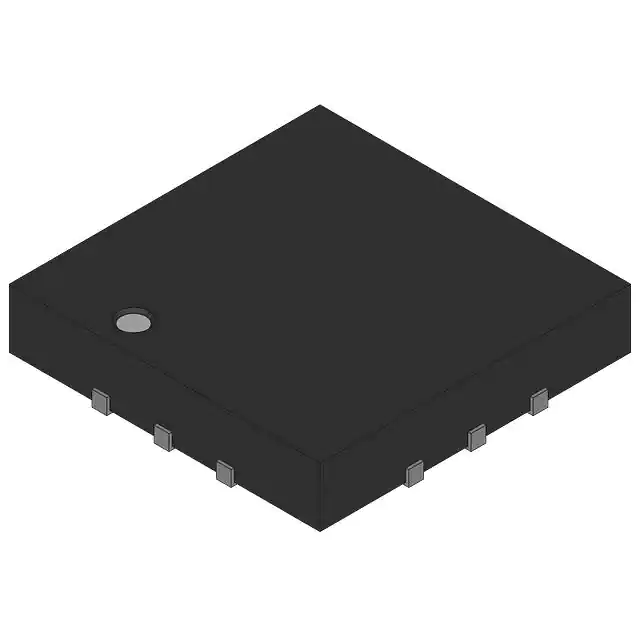
NXP Semiconductors FXLN8362QR1
- Part No.:
- FXLN8362QR1
- Manufacturer:
- NXP Semiconductors
- Category:
- Accelerometers
- Package:
- 12-VQFN Exposed Pad
- Datasheet:
-
 FXLN8362QR1.pdf
- Description:
- ACCELEROMETER 4-16G ANALOG 12QFN
- Quantity:
- Payment:

- Shipping:

Inventory:1,501
Please send an inquiry. Send us your inquiry, and we will respond immediately.
Product details
Overview
FXLN8362QR1 from NXP Semiconductors (formerly Freescale) is a 3-axis analog-output accelerometer with ±4 g / ±16 g full-scale range selection, low-power operation (180 µA typical active current), fixed 0.75 V zero-g output offset, and low-bandwidth configuration (1.1 kHz XY / 600 Hz Z). It serves as a motion-sensing front-end in tilt, vibration, and activity monitoring systems operating from –40 °C to +105 °C.
For engineers reviewing the FXLN8362QR1 datasheet, FXLN8362QR1 pinout, FXLN8362QR1 application, or FXLN8362QR1 equivalent, this page delivers verified technical context, validated pin functions, real-world use cases, and confirmed alternative options for industrial motion sensing designs requiring stable analog acceleration outputs and configurable g-range.
Technical Context
The FXLN8362QR1 integrates a MEMS acceleration sensor with a CMOS ASIC that provides internally compensated analog outputs for X, Y, and Z axes - each buffered and referenced to a supply-independent 0.75 V zero-g level. Its g-range is selected dynamically via the g-Select pin: logic high enables ±4 g mode (114.5 mV/g sensitivity), logic low enables ±16 g mode (28.62 mV/g).
Bandwidth is factory-configured to low mode (1.1 kHz on X/Y, 600 Hz on Z) and adjusted externally using 9.1 nF capacitors on all three output pins. The device supports self-test activation via ST pin and power management via EN pin, entering <30 nA shutdown current when EN is low.
Key Specifications
| Parameter | Value and Actual Design Meaning |
|---|---|
| Supply Voltage | 1.71 V to 3.6 V - compatible with single Li-ion, coin-cell, or 3.3 V rail without external regulation |
| Full-Scale Range | ±4 g or ±16 g - selected in-circuit via g-Select pin; enables dual-mode deployment in same hardware |
| Active Current | 180 µA typical - allows multi-year battery life in always-on motion detection nodes |
| Zero-G Output | 0.75 V ±45 mV - supply-independent reference simplifies ADC interfacing and eliminates ratiometric error |
| Output Bandwidth | 1.1 kHz (X/Y), 600 Hz (Z) - optimized for vibration analysis and slow-motion tilt sensing |
| Output Impedance | 10 kΩ typical - defines minimum load capacitance (9.1 nF) for stable bandwidth control |
| Operating Temp | –40 °C to +105 °C - qualified for white goods, industrial robotics, and automotive cabin applications |
Pinout & Package
FXLN8362QR1 uses a 3 mm × 3 mm × 1 mm, 12-pin QFN package (Case 2300-01, 0.65 mm pitch) with exposed pad (EP) not to be soldered. Pin 1 is marked by top-side dot; pin numbering follows standard counter-clockwise layout from top-left corner.
| Pin/Terminal | Circuit Role | Design Meaning |
|---|---|---|
| BYP | Internal regulator output capacitor node | Stabilizes internal 1.5 V regulator; requires 100 nF ceramic capacitor to GND for noise immunity |
| VDD | Main supply input | Accepts 1.71–3.6 V; must ramp before enabling EN to avoid startup failure |
| ST | Self-test control input | Logic high applies electrostatic actuation force - verifies sensor and signal path integrity without mechanical stimulus |
| EN | Power enable input | Logic low disables internal circuitry, reducing current to 30 nA; logic high enables full operation |
| g-Select | Full-scale range selector | High = ±4 g (114.5 mV/g); low = ±16 g (28.62 mV/g); transition delay ≤340 µs |
| GND (Pins 6 & 7) | Dual ground connections | Provides low-impedance return path for analog and digital sections; improves PSRR and noise rejection |
| ZOUT | Z-axis analog output | Buffered voltage output with 0.75 V zero-g offset; bandwidth set by external capacitor (9.1 nF) |
| YOUT | Y-axis analog output | Same zero-g offset and bandwidth configuration as ZOUT; independent of X/Y orientation |
| XOUT | X-axis analog output | Matches YOUT electrical behavior; all three outputs share identical DC offset and AC response tuning |
| NC (Pins 11 & 12) | No-connect terminals | May be left floating or tied to GND; no internal connection - no impact on performance or reliability |
Key Features
| Feature | Design Value |
|---|---|
| Supply-Independent Zero-G Offset | 0.75 V ±45 mV across 1.71–3.6 V VDD - eliminates need for ratiometric ADC or supply monitoring in low-cost systems |
| Dynamically Configurable Full-Scale Range | ±4 g / ±16 g selection via single logic-level g-Select pin - enables one BOM to serve multiple mechanical shock/vibration profiles |
| Low-Power Analog Interface | 180 µA active current with buffered 10 kΩ outputs - directly drives RC filters or 12-bit SAR ADCs without op-amp buffering |
| Integrated Self-Test | Electrostatic actuation on ST pin validates sensor integrity and analog chain - replaces manual calibration checks in production test |
| Robust Mechanical Rating | 10,000 g shock survivability - withstands board-level reflow, drop testing, and harsh industrial handling without parameter shift |
Applications
| Tamper Detection System | White Goods Tilt/Vibration Monitor |
|---|---|
Use Scenario: Detect unauthorized physical movement or enclosure opening in utility meters or secure enclosures. IC Role / Device Role / Timing Role: Analog acceleration front-end capturing low-frequency displacement events with ±16 g range for impact detection. Use Value: Enables reliable tamper flag generation using only the FXLN8362QR1's self-test and g-Select pin - no external comparator or microcontroller required for basic alerting. |
Use Scenario: Monitor drum imbalance, door closure angle, or transport-induced vibration in washing machines and dryers. IC Role / Device Role / Timing Role: Low-bandwidth (1.1 kHz XY / 600 Hz Z) analog sensor feeding MCU ADC for real-time tilt and shake classification. Use Value: Fixed 0.75 V zero-g offset ensures consistent baseline across temperature and supply variation - critical for repeatable threshold-based diagnostics. |
| Industrial Robotics Inclinometer | Sports Activity Tracker |
Use Scenario: Measure joint angle or platform inclination in collaborative robot end-effectors or mobile base leveling systems. IC Role / Device Role / Timing Role: High-accuracy ±4 g analog output source with <±2 mg/°C zero-g drift - used for static tilt calculation via arctangent of X/Z or Y/Z ratios. Use Value: 114.5 mV/g sensitivity at ±4 g provides >10-bit effective resolution with 12-bit ADC - sufficient for <0.1° tilt resolution over ±30° range. |
Use Scenario: Capture repetitive motion patterns (walking, running, cycling) in wearable fitness bands or medical rehab devices. IC Role / Device Role / Timing Role: Low-current (180 µA) analog motion sensor operating from coin cell, with ±16 g range for impact event capture during falls or jumps. Use Value: Dual g-range capability allows same firmware to interpret both subtle gait dynamics (±4 g) and high-impact events (±16 g) - reducing sensor count per device. |
Equivalent & Alternatives
The following parts are listed as comparable options for similar analog-output accelerometer applications.
| Alternative Part | Technical Difference | Application Difference | Selection Advice |
|---|---|---|---|
| FXLN8372QR1 | Same package and pinout; high-bandwidth mode (2.7 kHz XY / 600 Hz Z) factory-configured; otherwise identical electrical interface and g-range options | Required for higher-frequency vibration analysis (e.g., motor bearing fault detection) where 1.1 kHz limit of FXLN8362QR1 is insufficient | Select FXLN8372QR1 only if system demands >1.1 kHz XY bandwidth; no PCB change needed but external capacitor values differ (8.2 nF on Z, 3.3 nF on X/Y) |
| MMA8452QT | Digital I²C output; 12-bit resolution; ±2/±4/±8 g ranges; 200 µA active current; lacks analog outputs and fixed zero-g offset | Suitable for microcontroller-based systems with I²C interface and onboard digital filtering; not drop-in for analog-signal-chain designs | Choose MMA8452QT when digital integration, embedded FIFO, or motion detection interrupts are required - not for direct replacement of FXLN8362QR1's analog interface |
Compared with FXLN8362QR1, FXLN8372QR1 offers higher XY bandwidth with identical pinout and analog interface, while MMA8452QT shifts to digital I²C output and removes the supply-independent 0.75 V reference - making it incompatible for analog-signal-path continuity but advantageous for firmware-controlled motion processing.
Availability
FXLN8362QR1 is available at Aetrix Electronics and suitable for white goods tilt sensing, industrial robotics inclinometry, and sports activity monitoring requiring stable component supply, long-term lifecycle support, and RoHS-compliant QFN packaging.
Supply support for FXLN8362QR1 includes scheduled delivery planning, volume procurement assistance, BOM continuity management, traceable sourcing, and lifecycle availability coordination for OEM customers, industrial embedded developers, connected-device designers, and electronics production programs.
Manufacturer
NXP Semiconductors acquired Freescale in 2015 and continues development of the Xtrinsic sensor portfolio, focusing on intelligent, low-power sensing solutions for industrial, automotive, and IoT applications.
The FXLN8362QR1 belongs to the Xtrinsic FXLN83xxQ family - designed specifically for cost-sensitive, battery-operated motion sensing applications requiring analog outputs, configurable g-ranges, and robust mechanical reliability without digital interface overhead.
FAQ
What is the full-scale range configuration method for FXLN8362QR1?
The FXLN8362QR1 supports ±4 g and ±16 g full-scale ranges selected dynamically via its g-Select pin: logic high configures ±4 g (114.5 mV/g sensitivity), logic low configures ±16 g (28.62 mV/g). This selection is active immediately after g-Select transition, with ≤340 µs settling time. No register writes or external programming are required - the function is purely hardware-controlled and fully supported in the FXLN8362QR1 datasheet Rev 2.0.
Does FXLN8362QR1 require external decoupling capacitors, and if so, what values?
Yes, FXLN8362QR1 requires three external capacitors: a 100 nF ceramic capacitor between BYP and GND to stabilize the internal 1.5 V regulator; and 9.1 nF capacitors on XOUT, YOUT, and ZOUT to configure its low-bandwidth mode (1.1 kHz XY / 600 Hz Z). These values are specified in Table 5 of the FXLN8362QR1 datasheet and are mandatory for achieving rated bandwidth and noise performance.
How does the self-test function operate on FXLN8362QR1?
The FXLN8362QR1 self-test activates when the ST pin is driven logic high, applying an electrostatic actuation force to the MEMS sensor - simulating a known acceleration without mechanical stimulus. This produces a measurable output shift (35 mg on X/Y, 300 mg on Z) that verifies sensor integrity and analog signal chain functionality. The test is fully documented in Section 1.2 of the FXLN8362QR1 datasheet and requires no external equipment beyond a logic-level signal source.
What is the significance of the fixed 0.75 V zero-g output in FXLN8362QR1?
The FXLN8362QR1's fixed 0.75 V zero-g output is supply-independent - it remains stable across the full 1.71–3.6 V VDD range. This eliminates ratiometric errors common in analog sensors tied to VDD-referenced ADCs, simplifying signal conditioning and enabling accurate tilt or static acceleration measurement even with varying battery voltage. The specification is guaranteed over temperature (±45 mV) and is a core differentiator versus non-compensated accelerometers.
Can FXLN8362QR1 be used in automotive applications?
Yes, FXLN8362QR1 is qualified for operation from –40 °C to +105 °C and features 10,000 g shock survivability - meeting key environmental requirements for under-hood and cabin automotive subsystems such as seat position sensing, battery pack vibration monitoring, or ADAS-related motion feedback. While not AEC-Q200 certified, its thermal and mechanical specs align with many Tier-2 automotive use cases where full qualification is not mandated.
FXLN8362QR1 Specifications
- Product attributes
- Attribute value
- Manufacturer:
- NXP Semiconductors
- Series:
- Xtrinsic
- Package/Case:
- 12-VQFN Exposed Pad
- Packaging:
- Tape & Reel (TR)
- Product Status:
- Obsolete
- Type:
- Analog
- Axis:
- X, Y, Z
- Acceleration Range:
- ±4g, 16g
- Sensitivity (LSB/g):
- -
- Sensitivity (mV/g):
- 114.5 (±4g) ~ 28.62 (±16g)
- Bandwidth:
- 1.1kHz (X,Y), 600Hz (Z)
- Output Type:
- Analog Voltage
- Voltage - Supply:
- 1.71V ~ 3.6V
- Features:
- Selectable Scale
- Operating Temperature:
- -40°C ~ 105°C
- Grade:
- -
- Qualification:
- -
- Mounting Type:
- Surface Mount
- Supplier Device Package:
- 12-QFN (3x3)
FXLN8362QR1 FAQ
1.How can I place an order for FXLN8362QR1 through Aetrix?
Please submit a Request for Quotation (RFQ) for FXLN8362QR1 on Aetrix. Our sales agent will provide a competitive quotation and guide you through the order confirmation once you accept the terms.
2.Are the price and stock information for FXLN8362QR1 reliable?
The price and inventory of FXLN8362QR1 are updated periodically and may fluctuate due to market conditions. Stock and pricing data are typically refreshed every 24 hours. Quotation validity for FXLN8362QR1 is usually 5 days.
3.What payment methods are accepted for FXLN8362QR1?
We accept Wire Transfer, PayPal, Credit Card, Western Union, MoneyGram, and Escrow for FXLN8362QR1 transactions.
Note: Certain payment methods may incur a processing fee.
4.How is shipping managed for FXLN8362QR1?
FXLN8362QR1 orders can be shipped via leading logistics carriers, including DHL, UPS, FedEx, TNT, or Registered Mail.
Once your FXLN8362QR1 order is processed, you will receive an email with the shipment details and tracking number.
Note: Tracking information may take up to 24 hours to appear. Express delivery typically takes 3–5 business days.
5.How can I obtain technical support or documentation for FXLN8362QR1?
For technical support, including FXLN8362QR1 datasheets, pinout diagrams, or application guidance, please contact our engineering support team. They can provide detailed documentation and assistance for your FXLN8362QR1 requirements.
6.How does Aetrix verify that FXLN8362QR1 is sourced from the original manufacturer or authorized distributors?
All FXLN8362QR1 products on Aetrix are procured from qualified distributors and authorized channels. Our dedicated quality assurance team conducts strict verification, including traceability checks and, if necessary, third-party testing. This ensures that FXLN8362QR1 meets industry standards.
7.What is the process for return or replacement of FXLN8362QR1?
All FXLN8362QR1 units undergo pre-shipment inspection (PSI). If there is an issue with FXLN8362QR1, returns or replacements are accepted under the following conditions:
1.Quantity discrepancies, incorrect items, or visible external defects (such as breakage or corrosion), acknowledged by Aetrix.
2.The issue is reported within 90 days of delivery.
3.The FXLN8362QR1 part is unused and in its original packaging.
Return procedure for FXLN8362QR1:
1.Submit a request within 90 days.
2.Obtain a Return Material Authorization (RMA) from Aetrix.
FXLN8362QR1 Tags

-
MXC4005XC
Memsic Inc.

-
MC3419
Memsic Inc.

-
MC3479
Memsic Inc.

-
MXC6655XA
Memsic Inc.

-
MC3630
Memsic Inc.
.jpg)
-
LIS2HH12TR
STMicroelectronics

-
KX122-1037
Kionix Inc.
-
LIS2DE12TR
STMicroelectronics
-
LIS2DH12TR
STMicroelectronics

-
MC3635
Memsic Inc.
-
LIS2DS12TR
STMicroelectronics

-
LIS3DHTR
STMicroelectronics
Tech Hub

A practical engineering guide to 3.3V and 5V logic compatibility, input thresholds, resistor dividers, translator ICs, MOSFET level shifting, I2C pull-ups, timing limits and power-sequencing risks.

The 74HC595 uses push-pull logic outputs, while the TPIC6B595 uses 50 V open-drain DMOS sinks for higher-power loads. This guide compares timing, current limits, 3.3 V interfacing, load wiring, thermal…

The 74HC595 converts serial data into eight stable parallel outputs. This guide covers pin functions, shift and storage timing, OE and MR behavior, drive-current limits, cascading, voltage compatibilit…

A technical comparison of level-sensitive latches and edge-triggered flip-flops, covering timing windows, setup and hold limits, master–slave operation, time borrowing, race-through, HDL inference and…

A D latch stores one bit while Enable controls when data can pass. This reference covers gate-level operation, truth tables, transparency, setup and hold timing, LE versus OE, common ICs and practical …

An SR latch stores one bit through cross-coupled feedback. This engineering reference covers NOR and NAND implementations, truth tables, forbidden-state recovery, gated operation, switch debouncing, fa…

Latch circuits retain one bit through feedback. This technical reference covers SR and D latches, truth tables, transparency, timing limits, latch-versus-flip-flop behavior, applications and common log…

An engineering guide to LED driver operation, constant-current and constant-voltage outputs, linear and switching topologies, dimming, IC selection, calculations, replacement compatibility, and fault c…

Operational amplifier guide covering op amp basics, feedback, ideal vs real op amps, common configurations, buffer circuits, offset, bias current, gain-bandwidth, slew rate, rail-to-rail limits and sel…

Jumper cables guide covering safe connection order, red and black clamp placement, final ground connection, cable gauge, length, clamp quality, copper vs CCA cables, jump starter comparison and battery…


