
 My Inquiry
 My Account


NXP Semiconductors FXLN8371QR1
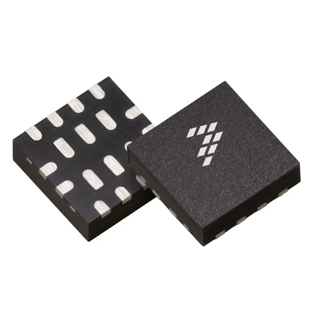
- Part No.:
- FXLN8371QR1
- Manufacturer:
- NXP Semiconductors
- Category:
- Accelerometers
- Package:
- 12-VQFN Exposed Pad
- Datasheet:
-
 FXLN8371QR1.pdf
- Description:
- ACCELEROMETER 2-8G ANALOG 12QFN
- Quantity:
- Payment:

- Shipping:

Inventory:2,206
Please send an inquiry. Send us your inquiry, and we will respond immediately.
Product details
Overview
FXLN8371QR1 from NXP (formerly Freescale) is a 3-axis analog-output accelerometer with ±2 g / ±8 g full-scale range selection, high-bandwidth output (2.7 kHz XY / 600 Hz Z), and ultra-low active current of 180 µA. It delivers internally compensated analog outputs (XOUT/YOUT/ZOUT) referenced to a fixed 0.75 V zero-g offset, operating from 1.71–3.6 V supply across –40 °C to +105 °C - used in white goods tilt detection and robotics motion sensing.
For engineers reviewing the FXLN8371QR1 datasheet, FXLN8371QR1 pinout, FXLN8371QR1 application, or FXLN8371QR1 equivalent, key selection criteria include its analog bandwidth configuration, g-range select logic, self-test capability, shutdown current (30 nA), and QFN-12 package compatibility with PCB layout constraints for shock-sensitive applications.
Technical Context
The FXLN8371QR1 integrates a MEMS acceleration sensor with a CMOS ASIC for signal conditioning, featuring independent analog output buffering per axis and factory-configured high-bandwidth mode. Its internal voltage regulator supplies a stable 1.5 V (±0.05 V) to the BYP pin, supporting external decoupling with 70–500 nF capacitors.
Full-scale range is selected via the g-Select pin: logic low enables ±8 g mode (sensitivity 57.25 mV/g), logic high enables ±2 g mode (229 mV/g). Self-test activation (ST pin high) applies electrostatic actuation to verify sensor and signal path integrity without mechanical stimulus.
Key Specifications
| Parameter | Value and Actual Design Meaning |
|---|---|
| Supply Voltage | 1.71–3.6 V - supports single-cell Li-ion or 3.3 V rail without level-shifting. |
| Active Current | 180 µA typical - enables multi-year battery life in activity monitors. |
| Shutdown Current | 30 nA - allows host MCU to disable sensor between measurements with negligible leakage. |
| Output Bandwidth | 2.7 kHz (X/Y), 600 Hz (Z) - optimized for vibration analysis and fast-motion capture. |
| Zero-g Offset | 0.75 V ±45 mV - fixed reference simplifies ADC scaling and eliminates supply-voltage dependency. |
| Noise Density | 200 µg/√Hz (X/Y), 280 µg/√Hz (Z) - defines minimum detectable acceleration in high-resolution applications. |
| Operating Temp | –40 °C to +105 °C - qualified for industrial motor control and automotive cabin environments. |
Pinout & Package
FXLN8371QR1 uses a 3 mm × 3 mm × 1 mm, 12-pin QFN package (Case 2300-01, 0.65 mm pitch) with exposed pad (EP) not to be soldered. Pin 1 is marked by dot; pins 11 and 12 are NC and may float or connect to GND.
| Pin/Terminal | Circuit Role | Design Meaning |
|---|---|---|
| BYP | Internal regulator output | Requires 70–500 nF capacitor to stabilize 1.5 V reference; powers internal analog circuitry. |
| VDD | Power supply input | 1.71–3.6 V main supply; must ramp before enabling EN to avoid startup failure. |
| ST | Self-test control | Logic high triggers electrostatic self-test; no mechanical stimulus needed for functional verification. |
| EN | Enable/shutdown | Logic low disables all analog outputs and reduces current to 30 nA; critical for power cycling. |
| g-Select | Full-scale range select | Logic high = ±2 g (229 mV/g); logic low = ±8 g (57.25 mV/g); transition delay 340 µs. |
| GND (pins 6 & 7) | Ground reference | Dual GND pins reduce ground impedance and improve noise immunity on analog outputs. |
| XOUT / YOUT / ZOUT | Analog acceleration outputs | Buffered, ratiometric outputs with 8–12 kΩ impedance; require external RC filtering for bandwidth tuning. |
Key Features
| Feature | Design Value |
|---|---|
| Factory-configured high-bandwidth mode | Enables 2.7 kHz XY response for real-time vibration monitoring without external configuration. |
| Fixed 0.75 V zero-g offset | Eliminates supply-voltage calibration drift and simplifies ADC reference selection in mixed-signal systems. |
| Electrostatic self-test (ST pin) | Verifies sensor integrity and signal chain functionality at power-on or during periodic diagnostics. |
| Robust mechanical design | Withstands 10,000 g shock - suitable for mounting on motors, compressors, and high-vibration appliances. |
| MSL 1 rating | Allows unlimited floor life and standard reflow without baking - reduces manufacturing overhead. |
Applications
| Tamper Detection | White Goods Tilt/Vibration Sensing |
|---|---|
Use Scenario: Detect unauthorized physical access or movement of secured enclosures (e.g., utility meters, kiosks). IC Role / Device Role / Timing Role: Analog-output accelerometer providing continuous low-power motion signature capture. Use Value: 30 nA shutdown current extends battery life to >5 years; ±8 g range captures impact events without clipping. |
Use Scenario: Monitor washing machine drum imbalance or refrigerator compressor vibration. IC Role / Device Role / Timing Role: High-bandwidth analog sensor feeding MCU ADC for real-time FFT-based fault analysis. Use Value: 2.7 kHz XY bandwidth resolves bearing harmonics; 10,000 g shock rating survives appliance transport and operation. |
| Robotics Motion Feedback | Inclinometer / Vibrometer |
Use Scenario: Provide orientation and dynamic motion feedback for collaborative robot end-effectors. IC Role / Device Role / Timing Role: Low-drift analog interface delivering precise tilt and acceleration data to motion controller. Use Value: 0.75 V zero-g offset and ±2 g mode (229 mV/g) enable sub-degree tilt resolution with 12-bit ADC. |
Use Scenario: Measure structural vibration amplitude/frequency in HVAC ducts or industrial machinery. IC Role / Device Role / Timing Role: Analog-output sensor with configurable bandwidth for spectral analysis of mechanical resonance. Use Value: Independent XY/Z bandwidth tuning (2.7 kHz vs. 600 Hz) isolates high-frequency vibration modes from gravity effects. |
Equivalent & Alternatives
The following parts are listed as comparable options for similar analog-output accelerometer applications.
| Alternative Part | Technical Difference | Application Difference | Selection Advice |
|---|---|---|---|
| FXLN8361QR1 | Same package and pinout; low-bandwidth mode (1.1 kHz XY / 600 Hz Z); identical ±2/±8 g range. | Better suited for low-frequency tilt or slow-motion detection where noise rejection outweighs speed. | Select FXLN8361QR1 when vibration frequency content is below 1 kHz and lower noise density (130 µg/√Hz) is prioritized. |
| ADXL326BCPZ | 3.3 V only supply; higher noise (220 µg/√Hz); fixed ±16 g range; no g-select or self-test. | Lacks programmable range and diagnostic features; requires external voltage regulation for 1.8–3.6 V systems. | Choose ADXL326BCPZ only if legacy design mandates ADI footprint compatibility and ±16 g range suffices. |
Compared with FXLN8361QR1, FXLN8371QR1 trades lower noise for higher XY bandwidth - critical for vibration analysis - while both share identical g-select logic and shutdown behavior. Against ADXL326BCPZ, FXLN8371QR1 offers wider supply range, integrated self-test, and selectable full-scale, but requires different external capacitor values for bandwidth tuning.
Availability
FXLN8371QR1 is available at Aetrix Electronics and suitable for white goods tilt detection, robotics motion feedback, and industrial inclinometer applications requiring stable component supply, long-term lifecycle support, and RoHS-compliant QFN packaging.
Supply support for FXLN8371QR1 includes scheduled delivery planning, volume procurement assistance, BOM continuity management, traceable sourcing, and lifecycle availability coordination for OEM customers, industrial embedded developers, connected-device designers, and electronics production programs.
Manufacturer
NXP Semiconductors acquired Freescale in 2015 and continues development of the Xtrinsic sensor portfolio, focusing on intelligent, low-power MEMS solutions for industrial and consumer applications.
The FXLN83xxQ series was designed specifically for cost-sensitive, battery-operated motion sensing in harsh environments - emphasizing analog output simplicity, shock survivability, and factory-configurable bandwidth without digital interfaces.
FAQ
What is the function of the BYP pin on the FXLN8371QR1?
The BYP pin on the FXLN8371QR1 provides the regulated 1.5 V output (±0.05 V) from the internal voltage regulator. It must be decoupled with a 70–500 nF capacitor to stabilize the analog signal chain. This pin supplies bias to internal circuitry and cannot be left floating; improper BYP capacitor selection causes output instability or increased noise in the FXLN8371QR1 analog outputs.
How does the g-Select pin configure full-scale range on the FXLN8371QR1?
On the FXLN8371QR1, the g-Select pin sets the full-scale range: logic high selects ±2 g (229 mV/g sensitivity), logic low selects ±8 g (57.25 mV/g). The transition delay is 340 µs, and the setting persists until changed. This dual-range capability allows one FXLN8371QR1 design to serve both precision tilt and high-g shock detection without hardware modification.
Can the FXLN8371QR1 operate from a 1.8 V supply?
Yes, the FXLN8371QR1 operates from 1.71 V to 3.6 V, making 1.8 V fully supported. At 1.8 V, the logic thresholds remain valid (VIH ≥ 1.35 V, VIL ≤ 0.54 V), and analog performance - including zero-g offset (0.75 V) and noise density - is maintained per characterization data. System designers can directly interface the FXLN8371QR1 with 1.8 V MCUs without level shifters.
What is the purpose of the ST (Self-Test) pin on the FXLN8371QR1?
The ST pin on the FXLN8371QR1 activates an electrostatic self-test that verifies sensor element integrity and analog signal path functionality without mechanical stimulation. When driven high, it induces a known acceleration-like response (35 mg on X/Y, 300 mg on Z), allowing firmware to validate sensor health at startup or during maintenance - a critical feature for safety-critical FXLN8371QR1 deployments.
Is the FXLN8371QR1 pin-compatible with FXLN8361QR1?
Yes, the FXLN8371QR1 is pin-compatible with FXLN8361QR1: identical 12-pin QFN-3×3 mm package, matching pin functions (VDD, GND, XOUT/YOUT/ZOUT, EN, ST, g-Select, BYP), and shared footprint. The only functional difference is factory-configured bandwidth - FXLN8371QR1 uses high-bandwidth mode (2.7 kHz XY), while FXLN8361QR1 uses low-bandwidth mode (1.1 kHz XY) - requiring no PCB changes for substitution.
FXLN8371QR1 Specifications
- Product attributes
- Attribute value
- Manufacturer:
- NXP Semiconductors
- Series:
- Xtrinsic
- Package/Case:
- 12-VQFN Exposed Pad
- Packaging:
- Tape & Reel (TR)
- Product Status:
- Obsolete
- Type:
- Analog
- Axis:
- X, Y, Z
- Acceleration Range:
- ±2g, 8g
- Sensitivity (LSB/g):
- -
- Sensitivity (mV/g):
- 229 (±2g) ~ 57.25 (±8g)
- Bandwidth:
- 2.7kHz (X,Y), 600Hz (Z)
- Output Type:
- Analog Voltage
- Voltage - Supply:
- 1.71V ~ 3.6V
- Features:
- Selectable Scale
- Operating Temperature:
- -40°C ~ 105°C
- Grade:
- -
- Qualification:
- -
- Mounting Type:
- Surface Mount
- Supplier Device Package:
- 12-QFN (3x3)
FXLN8371QR1 FAQ
1.How can I place an order for FXLN8371QR1 through Aetrix?
Please submit a Request for Quotation (RFQ) for FXLN8371QR1 on Aetrix. Our sales agent will provide a competitive quotation and guide you through the order confirmation once you accept the terms.
2.Are the price and stock information for FXLN8371QR1 reliable?
The price and inventory of FXLN8371QR1 are updated periodically and may fluctuate due to market conditions. Stock and pricing data are typically refreshed every 24 hours. Quotation validity for FXLN8371QR1 is usually 5 days.
3.What payment methods are accepted for FXLN8371QR1?
We accept Wire Transfer, PayPal, Credit Card, Western Union, MoneyGram, and Escrow for FXLN8371QR1 transactions.
Note: Certain payment methods may incur a processing fee.
4.How is shipping managed for FXLN8371QR1?
FXLN8371QR1 orders can be shipped via leading logistics carriers, including DHL, UPS, FedEx, TNT, or Registered Mail.
Once your FXLN8371QR1 order is processed, you will receive an email with the shipment details and tracking number.
Note: Tracking information may take up to 24 hours to appear. Express delivery typically takes 3–5 business days.
5.How can I obtain technical support or documentation for FXLN8371QR1?
For technical support, including FXLN8371QR1 datasheets, pinout diagrams, or application guidance, please contact our engineering support team. They can provide detailed documentation and assistance for your FXLN8371QR1 requirements.
6.How does Aetrix verify that FXLN8371QR1 is sourced from the original manufacturer or authorized distributors?
All FXLN8371QR1 products on Aetrix are procured from qualified distributors and authorized channels. Our dedicated quality assurance team conducts strict verification, including traceability checks and, if necessary, third-party testing. This ensures that FXLN8371QR1 meets industry standards.
7.What is the process for return or replacement of FXLN8371QR1?
All FXLN8371QR1 units undergo pre-shipment inspection (PSI). If there is an issue with FXLN8371QR1, returns or replacements are accepted under the following conditions:
1.Quantity discrepancies, incorrect items, or visible external defects (such as breakage or corrosion), acknowledged by Aetrix.
2.The issue is reported within 90 days of delivery.
3.The FXLN8371QR1 part is unused and in its original packaging.
Return procedure for FXLN8371QR1:
1.Submit a request within 90 days.
2.Obtain a Return Material Authorization (RMA) from Aetrix.
FXLN8371QR1 Tags

-
MXC4005XC
Memsic Inc.

-
MC3419
Memsic Inc.

-
MC3479
Memsic Inc.

-
MXC6655XA
Memsic Inc.

-
MC3630
Memsic Inc.
.jpg)
-
LIS2HH12TR
STMicroelectronics

-
KX122-1037
Kionix Inc.
-
LIS2DE12TR
STMicroelectronics
-
LIS2DH12TR
STMicroelectronics

-
MC3635
Memsic Inc.
-
LIS2DS12TR
STMicroelectronics

-
LIS3DHTR
STMicroelectronics
Tech Hub

A practical engineering guide to 3.3V and 5V logic compatibility, input thresholds, resistor dividers, translator ICs, MOSFET level shifting, I2C pull-ups, timing limits and power-sequencing risks.

The 74HC595 uses push-pull logic outputs, while the TPIC6B595 uses 50 V open-drain DMOS sinks for higher-power loads. This guide compares timing, current limits, 3.3 V interfacing, load wiring, thermal…

The 74HC595 converts serial data into eight stable parallel outputs. This guide covers pin functions, shift and storage timing, OE and MR behavior, drive-current limits, cascading, voltage compatibilit…

A technical comparison of level-sensitive latches and edge-triggered flip-flops, covering timing windows, setup and hold limits, master–slave operation, time borrowing, race-through, HDL inference and…

A D latch stores one bit while Enable controls when data can pass. This reference covers gate-level operation, truth tables, transparency, setup and hold timing, LE versus OE, common ICs and practical …

An SR latch stores one bit through cross-coupled feedback. This engineering reference covers NOR and NAND implementations, truth tables, forbidden-state recovery, gated operation, switch debouncing, fa…

Latch circuits retain one bit through feedback. This technical reference covers SR and D latches, truth tables, transparency, timing limits, latch-versus-flip-flop behavior, applications and common log…

An engineering guide to LED driver operation, constant-current and constant-voltage outputs, linear and switching topologies, dimming, IC selection, calculations, replacement compatibility, and fault c…

Operational amplifier guide covering op amp basics, feedback, ideal vs real op amps, common configurations, buffer circuits, offset, bias current, gain-bandwidth, slew rate, rail-to-rail limits and sel…

Jumper cables guide covering safe connection order, red and black clamp placement, final ground connection, cable gauge, length, clamp quality, copper vs CCA cables, jump starter comparison and battery…


