
 My Inquiry
 My Account


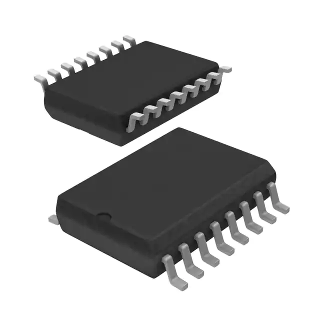
STMicroelectronics L3G4200DTR
- Part No.:
- L3G4200DTR
- Manufacturer:
- STMicroelectronics
- Category:
- Gyroscopes
- Package:
- 16-TFLGA
- Datasheet:
-
 L3G4200DTR.pdf
- Description:
- IC GYROSCOPE MEMS 3AXIS LP 16LGA
- Quantity:
- Payment:

- Shipping:

Inventory:1,892
Please send an inquiry. Send us your inquiry, and we will respond immediately.
Product details
Overview
L3G4200DTR from STMicroelectronics is a 3-axis digital gyroscope IC with I²C and SPI interfaces, ±250/±500/±2000 dps full-scale range selection, 16-bit data resolution, and embedded FIFO for motion sensing in compact portable devices. It operates from 2.4 V to 3.6 V, consumes 6.1 mA typical at 100 Hz ODR, and integrates self-test and temperature sensor functionality.
For engineers reviewing the L3G4200DTR datasheet, L3G4200DTR pinout, L3G4200DTR application, or L3G4200DTR equivalent, key selection criteria include angular rate accuracy over temperature, interface flexibility (I²C/SPI), low-power mode timing behavior, and FIFO buffer depth for burst-read efficiency in battery-powered inertial measurement units.
Technical Context
The L3G4200DTR implements a micromachined tuning-fork gyroscope structure with analog front-end amplification, 16-bit sigma-delta ADC conversion, and digital signal processing including high-pass filtering for motion artifact suppression. Its output data rate is programmable from 100 Hz to 800 Hz in normal mode.
It supports both I²C (up to 400 kHz) and 4-wire SPI (up to 10 MHz) communication protocols, with separate interrupt pins (INT1, INT2) configurable for data-ready, FIFO threshold, or wake-up events - enabling tight synchronization with host MCUs in wearable and handheld platforms.
Key Specifications
| Parameter | Value and Actual Design Meaning |
|---|---|
| Full-Scale Range | Configurable ±250/±500/±2000 dps - determines maximum measurable angular velocity without saturation |
| Output Data Rate | 100–800 Hz (normal mode) - sets sampling frequency for real-time motion tracking loop timing |
| Supply Voltage | 2.4 V to 3.6 V - compatible with single-cell Li-ion or regulated 3.3 V rails in portable systems |
| Current Consumption | 6.1 mA typical at 100 Hz ODR - enables >100-hour operation on 600 mAh battery in always-on motion detection |
| FIFO Depth | 32-level 16-bit samples per axis - reduces host polling overhead and preserves data during MCU sleep cycles |
| Interface | I²C (400 kHz) and 4-wire SPI (10 MHz) - allows coexistence with other sensors on shared bus or deterministic timing-critical reads |
| Operating Temperature | −40 °C to +85 °C - validated for consumer-grade indoor/outdoor portable electronics deployment |
Pinout & Package
Package: 16-pin LGA (3 mm × 3 mm × 0.85 mm), RoHS-compliant, exposed pad for thermal dissipation.
| Pin/Terminal | Circuit Role | Design Meaning |
|---|---|---|
| VDD | Power supply input | Connects to 2.4–3.6 V regulated rail; requires local 100 nF decoupling |
| GND | Ground reference | Common return path for analog/digital sections; tied to exposed pad |
| SCL/SPC | I²C clock / SPI clock | Shared pin: I²C SCL when SDO/SA0 = low; SPI SPC when SDO/SA0 = high |
| SDA/SDI | I²C data / SPI data in | Shared pin: bidirectional I²C data when SDO/SA0 = low; SPI MOSI when SDO/SA0 = high |
| SDO/SA0 | Interface select / I²C address LSB | High = SPI mode; low = I²C mode with 7-bit address 0x68 or 0x69 depending on SA0 state |
| CS | SPI chip select | Active-low enable for SPI transactions; must be held high for I²C operation |
| INT1 | Programmable interrupt 1 | Configurable for data-ready, FIFO threshold, or wake-up event; open-drain output |
| INT2 | Programmable interrupt 2 | Independent configuration from INT1; supports motion detection and status reporting |
| DRDY | Data ready indicator | Dedicated output (not multiplexed) signaling new sample availability in all interface modes |
Key Features
| Feature | Design Value |
|---|---|
| Embedded FIFO buffer | 32-sample depth per axis reduces host CPU load and enables low-power burst-read architecture |
| Self-test function | On-chip electrostatic actuation verifies mechanical integrity without external stimulus |
| Temperature sensor | Integrated 8-bit ADC provides on-die temperature reading for gyro bias compensation |
| High-pass filter | Configurable cut-off frequency removes static tilt offset from angular rate output |
| Wake-up detection | Hardware-accelerated motion-triggered interrupt wakes host MCU from deep-sleep states |
Applications
| Smartphone Motion UI | Wearable Fitness Tracker |
|---|---|
Use Scenario: Detecting device rotation for screen orientation lock/unlock and gesture-based navigation. IC Role / Device Role / Timing Role: Primary angular rate sensor feeding real-time orientation fusion algorithm with <10 ms latency. Use Value: ±250 dps FSR and 100 Hz ODR provide sufficient dynamic range and responsiveness for human-hand motion without oversampling overhead. | Use Scenario: Capturing arm swing amplitude and cadence during walking or running activities. IC Role / Device Role / Timing Role: Core motion engine triggering step-counting and activity classification via host MCU firmware. Use Value: FIFO buffering and wake-up interrupt reduce average current to <15 µA in motion-triggered duty cycling. |
| Remote-Control Pointer | VR/AR Headset Stabilization |
Use Scenario: Translating hand-held remote tilt into cursor movement on TV or display interface. IC Role / Device Role / Timing Role: Low-latency angular rate source synchronized with IR or Bluetooth transmission timing. Use Value: SPI interface supports deterministic 10 MHz read timing critical for sub-20 ms end-to-end pointer lag. | Use Scenario: Compensating for head rotation jitter during immersive visual rendering. IC Role / Device Role / Timing Role: High-bandwidth motion input (800 Hz ODR) feeding real-time IMU fusion stack. Use Value: ±2000 dps FSR accommodates rapid head turns while maintaining 16-bit resolution for fine stabilization control. |
Equivalent & Alternatives
The following parts are listed as comparable options for similar 3-axis digital gyroscope applications.
| Alternative Part | Technical Difference | Application Difference | Selection Advice |
|---|---|---|---|
| LSM6DS3TR | Integrated 3-axis accelerometer + gyroscope in same package; higher power (1.2 mA @ 100 Hz), I²C/SPI only | Reduces BOM count and PCB area vs. discrete sensor solution; requires co-location calibration | Select when system-level size and integration outweigh need for independent sensor replacement or calibration |
| ADXRS649 | Analog-output single-axis gyroscope; wider bandwidth (2.5 kHz), higher noise floor (0.015°/√Hz), ±2500 dps FSR | Used in industrial stabilization requiring analog feedback loop compatibility and high-frequency response | Select for closed-loop servo control where analog voltage output avoids ADC quantization and latency |
Compared with LSM6DS3TR and ADXRS649, the L3G4200DTR offers dedicated 3-axis digital gyroscope performance with minimal external components, lower power than integrated IMUs, and simpler interface than analog alternatives - making it optimal for cost-sensitive, space-constrained motion UI and activity monitoring designs.
Availability
L3G4200DTR is available at Aetrix Electronics and suitable for smartphone motion UI, wearable fitness tracker, and remote-control pointer applications requiring stable component supply and long-term production continuity.
Supply support for L3G4200DTR includes scheduled delivery planning, volume procurement assistance, BOM continuity management, traceable sourcing, and lifecycle availability coordination for OEM customers, industrial embedded developers, connected-device designers, and electronics production programs.
Manufacturer
STMicroelectronics is a global semiconductor leader headquartered in Geneva, Switzerland, designing and manufacturing microcontrollers, sensors, power management ICs, and analog/mixed-signal devices for industrial, automotive, and consumer markets.
The L3G4200DTR belongs to ST's iNEMO inertial module family, engineered specifically for ultra-low-power, high-accuracy motion sensing in battery-operated portable electronics - emphasizing interface flexibility, embedded intelligence (FIFO, interrupts), and robustness across consumer temperature ranges.
FAQ
What is the recommended decoupling capacitor for L3G4200DTR?
A 100 nF ceramic capacitor placed as close as possible to the VDD pin is required for stable operation. STMicroelectronics' AN4508 application note specifies this value based on internal regulator impedance and switching noise characterization across 100 Hz–1 kHz bandwidth. Larger bulk capacitance (e.g., 1 µF) may be added in parallel if board layout constraints prevent optimal placement of the 100 nF unit.
Does L3G4200DTR support automatic zero-rate level calibration?
No - the L3G4200DTR does not perform automatic on-the-fly zero-rate calibration. Offset compensation is achieved via factory-trimmed registers (OUT_X_L/OUT_X_H, etc.) and optional user-programmable offset correction values stored in CTRL_REG2. Real-time drift correction requires external host MCU implementation using temperature sensor output and lookup tables or adaptive filtering algorithms.
Can INT1 and INT2 be used simultaneously for different events?
Yes - INT1 and INT2 are independently configurable through CTRL_REG3 and CTRL_REG4. For example, INT1 can be set to trigger on data-ready events while INT2 signals FIFO threshold overflow. Both outputs are open-drain and require external pull-up resistors; simultaneous assertion is electrically valid and supported in all interface modes per ST's L3G4200D datasheet revision 5.
Is the L3G4200DTR qualified for automotive applications?
No - the L3G4200DTR is specified for industrial and consumer temperature ranges (−40 °C to +85 °C) and is not AEC-Q100 qualified. STMicroelectronics offers the L3GD20H variant for automotive use, which includes extended qualification, enhanced ESD tolerance (±8 kV HBM), and production traceability per IATF 16949. Use of L3G4200DTR in safety-critical vehicle systems is not supported.
L3G4200DTR Specifications
- Product attributes
- Attribute value
- Manufacturer:
- STMicroelectronics
- Series:
- -
- Package/Case:
- 16-TFLGA
- Packaging:
- Tape & Reel (TR)
- Product Status:
- Obsolete
- Type:
- Digital
- Axis:
- X (Pitch), Y (Roll), Z (Yaw)
- Range °/s:
- ±250, 500, 2000
- Sensitivity (LSB/(°/s)):
- 8.75 ~ 70
- Sensitivity (mV/°/s):
- -
- Bandwidth:
- 100Hz ~ 800Hz
- Output Type:
- I2C, SPI
- Voltage - Supply:
- 2.4V ~ 3.6V
- Current - Supply:
- 6.1 mA
- Features:
- Adjustable Bandwidth, Selectable Scale, Sleep Mode, Temperature Sensor
- Operating Temperature:
- -40°C ~ 85°C
- Grade:
- -
- Qualification:
- -
L3G4200DTR FAQ
1.How can I place an order for L3G4200DTR through Aetrix?
Please submit a Request for Quotation (RFQ) for L3G4200DTR on Aetrix. Our sales agent will provide a competitive quotation and guide you through the order confirmation once you accept the terms.
2.Are the price and stock information for L3G4200DTR reliable?
The price and inventory of L3G4200DTR are updated periodically and may fluctuate due to market conditions. Stock and pricing data are typically refreshed every 24 hours. Quotation validity for L3G4200DTR is usually 5 days.
3.What payment methods are accepted for L3G4200DTR?
We accept Wire Transfer, PayPal, Credit Card, Western Union, MoneyGram, and Escrow for L3G4200DTR transactions.
Note: Certain payment methods may incur a processing fee.
4.How is shipping managed for L3G4200DTR?
L3G4200DTR orders can be shipped via leading logistics carriers, including DHL, UPS, FedEx, TNT, or Registered Mail.
Once your L3G4200DTR order is processed, you will receive an email with the shipment details and tracking number.
Note: Tracking information may take up to 24 hours to appear. Express delivery typically takes 3–5 business days.
5.How can I obtain technical support or documentation for L3G4200DTR?
For technical support, including L3G4200DTR datasheets, pinout diagrams, or application guidance, please contact our engineering support team. They can provide detailed documentation and assistance for your L3G4200DTR requirements.
6.How does Aetrix verify that L3G4200DTR is sourced from the original manufacturer or authorized distributors?
All L3G4200DTR products on Aetrix are procured from qualified distributors and authorized channels. Our dedicated quality assurance team conducts strict verification, including traceability checks and, if necessary, third-party testing. This ensures that L3G4200DTR meets industry standards.
7.What is the process for return or replacement of L3G4200DTR?
All L3G4200DTR units undergo pre-shipment inspection (PSI). If there is an issue with L3G4200DTR, returns or replacements are accepted under the following conditions:
1.Quantity discrepancies, incorrect items, or visible external defects (such as breakage or corrosion), acknowledged by Aetrix.
2.The issue is reported within 90 days of delivery.
3.The L3G4200DTR part is unused and in its original packaging.
Return procedure for L3G4200DTR:
1.Submit a request within 90 days.
2.Obtain a Return Material Authorization (RMA) from Aetrix.
L3G4200DTR Tags
-
I3G4250DTR
STMicroelectronics

-
IAM-20380HT
TDK InvenSense

-
IAM-20380
TDK InvenSense
-
A3G4250DTR
STMicroelectronics
-
SCR2100-D08-05
Murata Electronics
-
ADXRS623BBGZ-RL
Analog Devices Inc.
-
ADXRS624BBGZ-RL
Analog Devices Inc.
-
ADXRS620BBGZ-RL
Analog Devices Inc.
-
ADXRS642BBGZ-RL
Analog Devices Inc.
-
ADXRS450BEYZ
Analog Devices Inc.
-
ADXRS453BRGZ
Analog Devices Inc.
-
ADXRS649BBGZ
Analog Devices Inc.
Tech Hub

A practical engineering and sourcing framework covering lifecycle verification, lifetime-buy calculations, replacement qualification, supplier checks and counterfeit-risk controls.

TTL and CMOS logic families differ in thresholds, loading, output drive, power and timing. This engineering guide compares 74HC and 74HCT, calculates noise margins and checks 3.3 V/5 V compatibility.

A practical engineering guide to 3.3V and 5V logic compatibility, input thresholds, resistor dividers, translator ICs, MOSFET level shifting, I2C pull-ups, timing limits and power-sequencing risks.

The 74HC595 uses push-pull logic outputs, while the TPIC6B595 uses 50 V open-drain DMOS sinks for higher-power loads. This guide compares timing, current limits, 3.3 V interfacing, load wiring, thermal…

The 74HC595 converts serial data into eight stable parallel outputs. This guide covers pin functions, shift and storage timing, OE and MR behavior, drive-current limits, cascading, voltage compatibilit…

A technical comparison of level-sensitive latches and edge-triggered flip-flops, covering timing windows, setup and hold limits, master–slave operation, time borrowing, race-through, HDL inference and…

A D latch stores one bit while Enable controls when data can pass. This reference covers gate-level operation, truth tables, transparency, setup and hold timing, LE versus OE, common ICs and practical …

An SR latch stores one bit through cross-coupled feedback. This engineering reference covers NOR and NAND implementations, truth tables, forbidden-state recovery, gated operation, switch debouncing, fa…

Latch circuits retain one bit through feedback. This technical reference covers SR and D latches, truth tables, transparency, timing limits, latch-versus-flip-flop behavior, applications and common log…

An engineering guide to LED driver operation, constant-current and constant-voltage outputs, linear and switching topologies, dimming, IC selection, calculations, replacement compatibility, and fault c…


