
 My Inquiry
 My Account


STMicroelectronics LIS3L02DQ
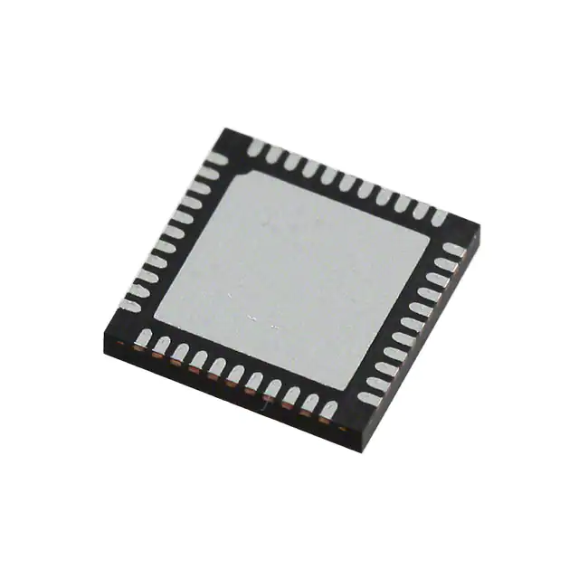
- Part No.:
- LIS3L02DQ
- Manufacturer:
- STMicroelectronics
- Category:
- Accelerometers
- Package:
- 44-QFN
- Datasheet:
-
 LIS3L02DQ.pdf
- Description:
- ACCELEROMETER 2G I2C/SPI 44QFN
- Quantity:
- Payment:

- Shipping:

Inventory:4,563
Please send an inquiry. Send us your inquiry, and we will respond immediately.
Product details
Overview
LIS3L02DQ from STMicroelectronics is a 3-axis ±2g digital output linear accelerometer with 12-bit resolution, I²C/SPI serial interface, and motion-activated interrupt capability. It delivers factory-trimmed sensitivity (1024 LSB/g typ.), operates from 2.7V to 3.6V, and supports 1.8V I/O compatibility-enabling direct interfacing with low-voltage microcontrollers in portable motion-sensing applications.
For engineers reviewing the LIS3L02DQ datasheet, LIS3L02DQ pinout, LIS3L02DQ application, or LIS3L02DQ equivalent, key selection criteria include its programmable interrupt threshold, embedded self-test function, shock survivability (10,000g), digital filter bandwidth control via decimation factor, and QFN-44 package footprint for space-constrained PCB layouts.
Technical Context
The LIS3L02DQ integrates a surface-micromachined capacitive MEMS sensing element with a CMOS IC interface featuring three ΣΔ analog-to-digital converters (one per axis), reconstruction filters, and configurable digital output data rates (280 Hz to 4.48 kHz). Its charge amplifier and ΣΔ modulators operate at 107.5 kHz and 35.8 kHz respectively, enabling high-resolution DC-coupled acceleration measurement.
Factory calibration trims gain, offset, common mode, and internal clock frequency into nonvolatile memory, eliminating need for user calibration. The RDY/INT pin provides synchronous data-ready signaling or inertial wake-up interrupts triggered when acceleration exceeds a user-defined threshold on any axis.
Key Specifications
| Parameter | Value and Actual Design Meaning |
|---|---|
| Acceleration Range | ±2 g - Full-scale range optimized for human-motion detection and tilt sensing without saturation. |
| Resolution | 12-bit - Delivers 0.97 mg/LSB (4 g / 4096), enabling sub-millig-level motion discrimination. |
| Sensitivity | 1024 LSB/g (typ.) - Factory-trimmed value ensures consistent scaling across units without post-manufacture calibration. |
| Output Data Rate | 280–4480 Hz - Configurable via decimation factor (8–128), supporting both low-power monitoring and high-speed vibration analysis. |
| Digital Filter BW | 70–1120 Hz (−3 dB) - Matches output rate settings to suppress aliasing while preserving signal fidelity. |
| Supply Voltage | 2.7–3.6 V - Compatible with single-cell Li-ion and regulated 3.3 V rails; I/O pads support 1.8 V logic levels. |
| Power-Down Current | 15 µA - Enables battery-operated devices to extend runtime during idle periods. |
Pinout & Package
Package: QFN-44, 7 mm × 7 mm × 1 mm, lead-free and RoHS-compliant (ECO-PACK®). Exposed thermal pad recommended for grounding to improve thermal performance and mechanical stability.
| Pin/Terminal | Circuit Role | Design Meaning |
|---|---|---|
| 1–2, 5–12, 23–44 | NC | Internally not connected - Must remain unconnected; no pull-up/down required. |
| 3, 22 | GND | 0 V reference for analog and digital sections - Requires low-impedance connection to PCB ground plane. |
| 4, 21 | Vdd | Analog/digital core supply (2.7–3.6 V) - Decoupled with 100 nF ceramic + 10 µF aluminum capacitor. |
| 13 | Reserved | Leave unconnected or tie to Vdd_IO - Not functional; avoid floating. |
| 14 | Reserved | Leave unconnected or tie to GND - Not functional; avoid floating. |
| 15 | RDY/INT | Open-drain interrupt/data-ready output - Signals new sample availability or motion-triggered wake-up event. |
| 16 | SDO | SPI serial data output - Driven only during SPI read cycles; tri-stated otherwise. |
| 17 | SDA/SDI/SDO | Multi-function pin: I²C SDA / SPI SDI / 3-wire SDO - Mode selected by CS state and CTRL_REG2 bit SIM. |
| 18 | SCL/SPC | I²C clock / SPI port clock - Shared physical terminal; timing governed by interface protocol. |
| 19 | CS | SPI enable / I²C mode select - High = I²C mode; Low = SPI mode; must be stable before communication. |
| 20 | Vdd_IO | I/O pad supply (1.8 V to Vdd+0.1 V) - Sets logic voltage level; decouple independently from Vdd. |
Key Features
| Feature | Design Value |
|---|---|
| Embedded Self-Test | Electrostatic actuation verifies mechanical integrity and signal chain functionality without external equipment. |
| Programmable Interrupt Threshold | User-configurable acceleration trigger on any axis enables low-power wake-up without host polling. |
| Factory Calibration | Gain, offset, and clock trimmed and stored in nonvolatile memory - eliminates system-level calibration effort. |
| High Shock Survivability | Rated for 10,000 g (0.1 ms) - Suitable for drop-prone consumer electronics and industrial handhelds. |
| Dual Interface Support | Single-pin-mapped I²C (400 kHz Fast Mode) and SPI (up to 8 MHz) - Simplifies integration across MCU platforms. |
Applications
| Mobile Device Motion Control | Industrial Vibration Monitoring |
|---|---|
|
Use Scenario: Detecting orientation changes, shake gestures, and free-fall events in smartphones and tablets. IC Role / Device Role / Timing Role: Primary 3-axis motion sensor providing real-time acceleration data to application processor via I²C. Use Value: Enables screen rotation, step counting, and UI interaction with <1.0 mg noise floor and guaranteed ±2g full-scale range. |
Use Scenario: Continuous monitoring of motor housing vibration in predictive maintenance systems. IC Role / Device Role / Timing Role: Edge-sensing node capturing broadband acceleration waveforms up to 1.12 kHz bandwidth. Use Value: Supports FFT-based spectral analysis with 12-bit resolution and programmable ODR to balance power vs. frequency content. |
| Anti-Theft Tilt Detection | Gaming Input Device |
|
Use Scenario: Triggering alarm when unauthorized movement or tilting exceeds threshold in asset tracking units. IC Role / Device Role / Timing Role: Low-power inertial wake-up source that activates MCU only upon tamper event. Use Value: Achieves <15 µA standby current and configurable interrupt latency (<6/ODR ms) for rapid response. |
Use Scenario: Translating hand motion into real-time 3D input for VR controllers and gesture-based interfaces. IC Role / Device Role / Timing Role: High-bandwidth motion capture sensor feeding raw acceleration data to motion fusion algorithm. Use Value: Delivers 4.48 kHz ODR and <0.3% FS nonlinearity (X/Y) to preserve spatial accuracy in immersive environments. |
Equivalent & Alternatives
The following parts are listed as comparable options for similar 3-axis ±2g digital accelerometer applications.
| Alternative Part | Technical Difference | Application Difference | Selection Advice |
|---|---|---|---|
| ADXL345 | 13-bit resolution, 2.0–3.6 V supply, I²C/SPI, no Vdd_IO separation - lacks dedicated I/O voltage rail. | Higher resolution but no 1.8 V I/O compatibility; requires level-shifting for 1.8 V MCUs. | Prefer ADXL345 when higher resolution and activity/inactivity detection are prioritized over I/O voltage flexibility. |
| LIS3DH | 12-bit resolution, ±2/±4/±8/±16 g ranges, 1.71–3.6 V supply, embedded FIFO, lower power-down current (0.5 µA). | Wider dynamic range selection and deeper FIFO simplify burst-mode acquisition in wearables. | Prefer LIS3DH when multi-range operation, ultra-low-power sleep, or onboard FIFO buffering are required. |
Compared with ADXL345 and LIS3DH, the LIS3L02DQ offers unique 1.8 V I/O compatibility and factory-trimmed calibration without requiring external compensation, making it optimal for cost-sensitive, space-constrained designs where fixed ±2g range suffices.
Availability
LIS3L02DQ is available at Aetrix Electronics and suitable for mobile device motion control, industrial vibration monitoring, anti-theft tilt detection, and gaming input device applications requiring stable component supply and long-term production continuity.
Supply support for LIS3L02DQ includes scheduled delivery planning, volume procurement assistance, BOM continuity management, traceable sourcing, and lifecycle availability coordination for OEM customers, industrial embedded developers, connected-device designers, and electronics production programs.
Manufacturer
STMicroelectronics is a global semiconductor leader headquartered in Geneva, Switzerland, designing and manufacturing microcontrollers, sensors, power management ICs, and automotive-grade components.
The LIS3L02DQ belongs to ST's legacy MEMS accelerometer family targeting cost-effective, high-reliability motion sensing in consumer and industrial edge devices - emphasizing robustness, ease of integration, and minimal calibration overhead.
FAQ
What is the maximum shock survivability rating for the LIS3L02DQ?
The LIS3L02DQ is rated for 10,000 g for 0.1 ms and 3,000 g for 0.5 ms under powered and unpowered conditions. This specification reflects mechanical robustness of the MEMS structure and packaging, validated per JEDEC standards - critical for handheld and portable equipment subject to drop impact.
Does the LIS3L02DQ require external calibration after soldering?
No. The LIS3L02DQ undergoes full factory calibration for gain, offset, common mode, and internal clock frequency, with trimming values stored in nonvolatile memory. Upon power-up, these parameters are automatically loaded - enabling plug-and-play operation without user calibration, even after PCB assembly stress.
How does the RDY/INT pin function in dual-role mode?
The RDY/INT pin operates as an open-drain output that can be configured either as a data-ready indicator (asserted each time new acceleration data is available) or as an inertial wake-up interrupt (triggered when acceleration exceeds a programmable threshold on any axis). Configuration is controlled via CTRL_REG1 register bits.
What is the significance of separate Vdd and Vdd_IO supplies?
Vdd powers the analog sensor core and digital logic, while Vdd_IO independently supplies the I/O buffer circuitry - allowing direct interface with 1.8 V microcontrollers without level shifters. This separation prevents noise coupling from digital switching into the analog path and ensures reliable communication across mixed-voltage systems.
LIS3L02DQ Specifications
- Product attributes
- Attribute value
- Manufacturer:
- STMicroelectronics
- Series:
- -
- Package/Case:
- 44-QFN
- Packaging:
- Tray
- Product Status:
- Obsolete
- Type:
- Digital
- Axis:
- X, Y, Z
- Acceleration Range:
- ±2g
- Sensitivity (LSB/g):
- -
- Sensitivity (mV/g):
- 1024
- Bandwidth:
- 70Hz ~ 1.12kHz
- Output Type:
- I2C, SPI
- Voltage - Supply:
- 2.7V ~ 3.6V
- Features:
- Adjustable Bandwidth
- Operating Temperature:
- -20°C ~ 70°C
- Grade:
- -
- Qualification:
- -
- Mounting Type:
- Surface Mount
- Supplier Device Package:
- 44-QFN-EP (7x7)
LIS3L02DQ FAQ
1.How can I place an order for LIS3L02DQ through Aetrix?
Please submit a Request for Quotation (RFQ) for LIS3L02DQ on Aetrix. Our sales agent will provide a competitive quotation and guide you through the order confirmation once you accept the terms.
2.Are the price and stock information for LIS3L02DQ reliable?
The price and inventory of LIS3L02DQ are updated periodically and may fluctuate due to market conditions. Stock and pricing data are typically refreshed every 24 hours. Quotation validity for LIS3L02DQ is usually 5 days.
3.What payment methods are accepted for LIS3L02DQ?
We accept Wire Transfer, PayPal, Credit Card, Western Union, MoneyGram, and Escrow for LIS3L02DQ transactions.
Note: Certain payment methods may incur a processing fee.
4.How is shipping managed for LIS3L02DQ?
LIS3L02DQ orders can be shipped via leading logistics carriers, including DHL, UPS, FedEx, TNT, or Registered Mail.
Once your LIS3L02DQ order is processed, you will receive an email with the shipment details and tracking number.
Note: Tracking information may take up to 24 hours to appear. Express delivery typically takes 3–5 business days.
5.How can I obtain technical support or documentation for LIS3L02DQ?
For technical support, including LIS3L02DQ datasheets, pinout diagrams, or application guidance, please contact our engineering support team. They can provide detailed documentation and assistance for your LIS3L02DQ requirements.
6.How does Aetrix verify that LIS3L02DQ is sourced from the original manufacturer or authorized distributors?
All LIS3L02DQ products on Aetrix are procured from qualified distributors and authorized channels. Our dedicated quality assurance team conducts strict verification, including traceability checks and, if necessary, third-party testing. This ensures that LIS3L02DQ meets industry standards.
7.What is the process for return or replacement of LIS3L02DQ?
All LIS3L02DQ units undergo pre-shipment inspection (PSI). If there is an issue with LIS3L02DQ, returns or replacements are accepted under the following conditions:
1.Quantity discrepancies, incorrect items, or visible external defects (such as breakage or corrosion), acknowledged by Aetrix.
2.The issue is reported within 90 days of delivery.
3.The LIS3L02DQ part is unused and in its original packaging.
Return procedure for LIS3L02DQ:
1.Submit a request within 90 days.
2.Obtain a Return Material Authorization (RMA) from Aetrix.
LIS3L02DQ Tags

-
MXC4005XC
Memsic Inc.

-
MC3419
Memsic Inc.

-
MC3479
Memsic Inc.

-
MXC6655XA
Memsic Inc.

-
MC3630
Memsic Inc.
.jpg)
-
LIS2HH12TR
STMicroelectronics

-
KX122-1037
Kionix Inc.
-
LIS2DE12TR
STMicroelectronics
-
LIS2DH12TR
STMicroelectronics

-
MC3635
Memsic Inc.
-
LIS2DS12TR
STMicroelectronics

-
LIS3DHTR
STMicroelectronics
Tech Hub

A practical engineering and sourcing framework covering lifecycle verification, lifetime-buy calculations, replacement qualification, supplier checks and counterfeit-risk controls.

TTL and CMOS logic families differ in thresholds, loading, output drive, power and timing. This engineering guide compares 74HC and 74HCT, calculates noise margins and checks 3.3 V/5 V compatibility.

A practical engineering guide to 3.3V and 5V logic compatibility, input thresholds, resistor dividers, translator ICs, MOSFET level shifting, I2C pull-ups, timing limits and power-sequencing risks.

The 74HC595 uses push-pull logic outputs, while the TPIC6B595 uses 50 V open-drain DMOS sinks for higher-power loads. This guide compares timing, current limits, 3.3 V interfacing, load wiring, thermal…

The 74HC595 converts serial data into eight stable parallel outputs. This guide covers pin functions, shift and storage timing, OE and MR behavior, drive-current limits, cascading, voltage compatibilit…

A technical comparison of level-sensitive latches and edge-triggered flip-flops, covering timing windows, setup and hold limits, master–slave operation, time borrowing, race-through, HDL inference and…

A D latch stores one bit while Enable controls when data can pass. This reference covers gate-level operation, truth tables, transparency, setup and hold timing, LE versus OE, common ICs and practical …

An SR latch stores one bit through cross-coupled feedback. This engineering reference covers NOR and NAND implementations, truth tables, forbidden-state recovery, gated operation, switch debouncing, fa…

Latch circuits retain one bit through feedback. This technical reference covers SR and D latches, truth tables, transparency, timing limits, latch-versus-flip-flop behavior, applications and common log…

An engineering guide to LED driver operation, constant-current and constant-voltage outputs, linear and switching topologies, dimming, IC selection, calculations, replacement compatibility, and fault c…


