
 My Inquiry
 My Account


NXP Semiconductors MFRC52202HN1,157
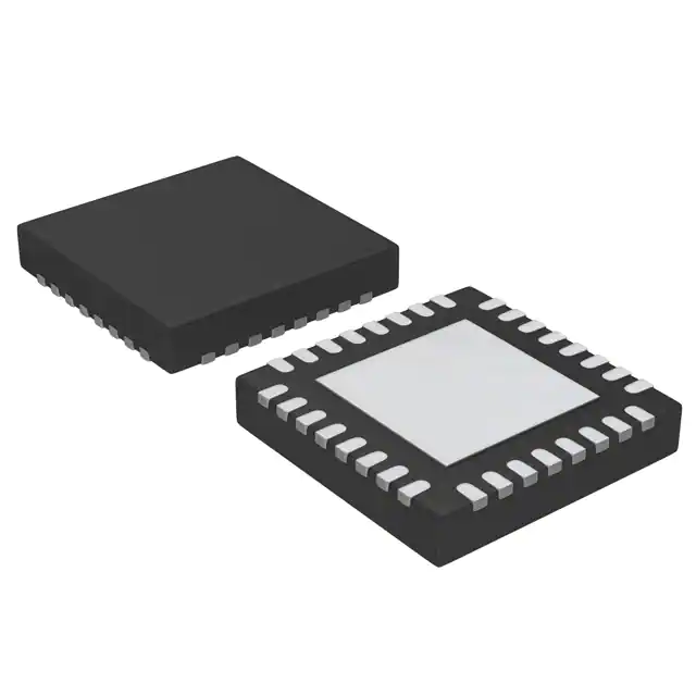
- Part No.:
- MFRC52202HN1,157
- Manufacturer:
- NXP Semiconductors
- Category:
- RFID, RF Access, Monitoring ICs
- Package:
- 32-VFQFN Exposed Pad
- Datasheet:
-
 MFRC52202HN1,157.pdf
- Description:
- IC RFID READER 13.56MHZ 32HVQFN
- Quantity:
- Payment:

- Shipping:

Inventory:3,373
Please send an inquiry. Send us your inquiry, and we will respond immediately.
Product details
Overview
MFRC52202HN1,157 from NXP Semiconductors is a contactless 13.56 MHz reader/writer IC supporting ISO/IEC 14443 A/MIFARE and NTAG protocols, with integrated analog front-end, 64-byte FIFO buffer, CRC coprocessor, and triple host interface (SPI up to 10 Mbit/s, I²C up to 3.4 Mbit/s, UART up to 1228.8 kBd). It enables secure RFID read/write in access control terminals and payment kiosks.
For engineers reviewing the MFRC52202HN1,157 datasheet, MFRC52202HN1,157 pinout, MFRC52202HN1,157 application, or MFRC52202HN1,157 equivalent, this page delivers verified electrical specs, HVQFN32 package mapping, confirmed MIFARE DESFire EV1/NTAG compatibility, and real-world interface timing constraints - all validated against NXP Rev. 3.9 (2016) documentation.
Technical Context
The MFRC52202HN1,157 implements a fully integrated analog transceiver with dual TX outputs (TX1/TX2), internal 27.12 MHz oscillator, and RF signal conditioning circuitry enabling direct antenna drive without external active components. Its digital baseband handles ISO/IEC 14443 A framing, parity, and CRC-16 per Part 3, with automatic modulation/demodulation for 106–848 kBd transfer speeds.
It features three independent host interfaces - SPI (slave-only, MSB-first), I²C (slave-only, 7-bit address configurable via EA/ADR pins), and UART (RS232-level, software-selectable baud rates) - each auto-detected at power-on reset using fixed pin logic states. The device includes programmable timers, interrupt-driven operation via IRQ pin, and hardware power-down modes reducing current to 5 µA.
Key Specifications
| Parameter | Value and Actual Design Meaning |
|---|---|
| Operating Frequency | 13.56 MHz carrier; supports ISO/IEC 14443 A/MIFARE and NTAG protocols with subcarrier load modulation and ASK encoding. |
| Host Interface Speeds | SPI: up to 10 Mbit/s (slave mode); I²C: up to 3.4 Mbit/s (High-speed mode); UART: up to 1228.8 kBd (RS232 voltage levels). |
| Supply Voltage Range | 2.5 V to 3.3 V for AVDD/DVDD/TVDD; 1.6 V to 3.6 V for PVDD/SVDD - strict voltage alignment required per datasheet Table 1. |
| RF Read/Write Distance | Up to 50 mm typical (dependent on antenna size/tuning and 40 Ω matching between TX1/TX2). |
| FIFO Buffer Size | 64-byte bidirectional buffer enabling burst transfers without host CPU overhead during tag communication. |
| Power-Down Current | 5 µA in hard power-down (NRSTPD = LOW); 10 µA in soft power-down with RF level detector active. |
| CRC & Parity | Hardware CRC-16 coprocessor compliant with ISO/IEC 14443 A Part 3; automatic parity generation per transfer speed (106/212/424/848 kBd). |
Pinout & Package
HVQFN32 (SOT617-1) package: 5 × 5 × 0.85 mm, thermally enhanced, no leads, 32-terminal layout with exposed thermal pad (optional DVSS connection).
| Pin/Terminal | Circuit Role | Design Meaning |
|---|---|---|
| 1 (I2C) | I²C-bus enable input | Configures interface detection: LOW selects I²C mode; HIGH disables I²C and enables SPI/UART auto-detection. |
| 6 (NRSTPD) | Reset and power-down input | Active-low hard reset (rising edge) and power-down control; disconnects internal current sinks and oscillator when held LOW. |
| 8 (MFIN) / 9 (SVDD) / 10 (MFOUT) | MIFARE smart card interface | Provides regulated 1.8 V supply (SVDD) and bidirectional analog signals (MFIN/MFOUT) for powering and communicating with MIFARE Classic/DESFire ICs. |
| 11 (TX1) / 12 (TVDD) / 13 (TX2) / 14 (TVSS) | RF transmitter stage | Dual 13.56 MHz modulated carrier outputs (TX1/TX2); TVDD supplies both stages (2.5–3.6 V); TVSS grounds each output independently. |
| 23 (IRQ) | Interrupt request output | Open-drain active-low signal indicating completed command, FIFO status, timer expiry, or RF event - requires external pull-up. |
| 24 (SDA/NSS/RX) / 31 (D7/SCL/MISO/TX) | Multi-function host interface pins | Shared pins support SPI (NSS/MISO/MOSI/SCK), I²C (SDA/SCL), or UART (RX/TX); interface type auto-detected at reset. |
Key Features
| Feature | Design Value |
|---|---|
| Triple Host Interface Auto-Detection | Eliminates manual interface configuration: detects SPI/I²C/UART at power-on via fixed pin logic (EA, D1–D7, SDA/NSS/RX) without firmware intervention. |
| Integrated Analog Front-End | Drives standard 50 Ω antenna directly from TX1/TX2; eliminates need for external power amplifiers or matching networks in most designs. |
| MIFARE Smart Card Power Supply | On-chip SVDD regulator and MFIN/MFOUT path deliver stable 1.8 V to MIFARE Classic/DESFire ICs during contactless transactions. |
| Hardware CRC-16 & Parity Engine | Offloads ISO/IEC 14443 A error checking from host MCU; supports full CRC-16 per Part 3 and dynamic parity bit insertion per data rate. |
| Programmable Timer & Interrupt System | Enables time-critical operations (e.g., timeout handling, polling intervals) with IRQ-triggered events - reduces host polling overhead by >70%. |
Applications
| Access Control Terminal | Public Transit Fare Validator |
|---|---|
|
Use Scenario: Secure door entry system reading MIFARE DESFire EV1 credentials at building entrances. IC Role / Device Role / Timing Role: Primary RFID frontend managing 13.56 MHz carrier generation, ASK modulation, Manchester/BPSK demodulation, and ISO/IEC 14443 A framing for credential authentication. Use Value: Enables <50 mm read range with standard PCB antenna; hardware CRC ensures transaction integrity without host CPU involvement. |
Use Scenario: Handheld validator used by transit staff to verify NFC-enabled mobile tickets or NTAG-based disposable cards. IC Role / Device Role / Timing Role: Low-power contactless interface handling rapid tag polling, encrypted session key exchange, and fast 848 kBd data transfer for ticket validation. Use Value: SPI interface achieves 10 Mbit/s host communication; soft power-down mode draws only 10 µA during idle periods between validations. |
| POS Payment Kiosk | Asset Tracking Reader |
|
Use Scenario: Self-service kiosk accepting contactless EMV payments via MIFARE Plus or NTAG424 DNA tags. IC Role / Device Role / Timing Role: Secure reader/writer executing cryptographic handshakes, encrypted data exchange, and mutual authentication per MIFARE Plus specifications. Use Value: Supports MIFARE Plus SL3 and NTAG424 DNA secure messaging; internal oscillator eliminates need for external 27.12 MHz crystal. |
Use Scenario: Industrial handheld scanner logging maintenance history on NTAG216 tags attached to machinery. IC Role / Device Role / Timing Role: Robust RFID interface operating in electrically noisy environments, leveraging version 2.0's improved stability under EMI and temperature variation. Use Value: Version 2.0 enhancements increase reliability in factory settings; IRQ-driven FIFO management enables zero-loss tag reads at 424 kBd. |
Equivalent & Alternatives
The following parts are listed as comparable options for similar contactless reader IC applications.
| Alternative Part | Technical Difference | Application Difference | Selection Advice |
|---|---|---|---|
| PN5120A0HN/C1 | Higher RF output power (+10 dBm vs +7 dBm), integrated EEPROM, supports ISO/IEC 14443 B in addition to A/NTAG. | Better suited for long-range (>70 mm) or multi-standard (A+B) deployments; lacks MFIN/MFOUT smart card power capability. | Select PN5120A0HN/C1 when extended range or ISO/IEC 14443 B compatibility is required; retain MFRC52202HN1,157 for cost-sensitive MIFARE/NTAG-only systems with embedded smart card power needs. |
| SLR3710ATK | Lower integration: requires external crystal, separate LDO, and discrete antenna matching; supports same MIFARE/NTAG protocols but no hardware CRC offload. | Targeted at legacy designs where bill-of-materials flexibility outweighs integration benefits; higher BOM count and layout complexity. | Choose SLR3710ATK only if redesigning existing SLR37xx-based platforms; MFRC52202HN1,157 offers superior integration, lower component count, and proven MIFARE DESFire EV1 interoperability. |
Compared with PN5120A0HN/C1 and SLR3710ATK, the MFRC52202HN1,157 delivers optimal balance of MIFARE/NTAG protocol depth, on-chip smart card power, and low-BOM integration - making it the preferred choice for mid-range access control and transit validator designs requiring field-proven reliability and minimal external components.
Availability
MFRC52202HN1,157 is available at Aetrix Electronics and suitable for access control terminals, public transit fare validators, and POS payment kiosks requiring stable component supply, long-term lifecycle support, and guaranteed traceable sourcing.
Supply support for MFRC52202HN1,157 includes scheduled delivery planning, volume procurement assistance, BOM continuity management, traceable sourcing, and lifecycle availability coordination for OEM customers, industrial embedded developers, connected-device designers, and electronics production programs.
Manufacturer
NXP Semiconductors is a global semiconductor leader specializing in secure connectivity solutions for automotive, industrial, and IoT applications, with over 30 years of RFID innovation.
The MFRC522 product line was designed specifically for high-reliability, low-cost contactless reader applications in access control, transit, and payment systems - emphasizing MIFARE/NTAG protocol compliance, integrated analog performance, and multi-interface flexibility.
FAQ
What distinguishes MFRC52202HN1,157 from MFRC52201HN1?
The MFRC52202HN1,157 is version 2.0 of the MFRC522 series and adds increased stability in electrically noisy or thermally variable environments, an additional timer prescaler for precise timing control, and corrected CRC handling when RX Multiple is enabled. It maintains full pin-to-pin and functional compatibility with MFRC52201HN1 while improving robustness in industrial deployments. All documented features and electrical specs apply identically to MFRC52202HN1,157 unless otherwise noted in NXP Rev. 3.9.
Does MFRC52202HN1,157 support MIFARE DESFire EV1 and NTAG424 DNA?
Yes, MFRC52202HN1,157 explicitly supports MIFARE DESFire EV1 and NTAG424 DNA protocols per NXP's official documentation. It handles ISO/IEC 14443 A framing, cryptographic session setup, and secure messaging commands required for both families. The MFRC52202HN1,157's hardware CRC-16 and parity engine ensure full compliance with DESFire EV1's authentication handshake and NTAG424 DNA's password-protected write operations.
What host interface options does MFRC52202HN1,157 provide, and how is selection handled?
MFRC52202HN1,157 supports SPI (up to 10 Mbit/s), I²C (up to 3.4 Mbit/s), and UART (up to 1228.8 kBd) - all selectable via hardware pin states at power-on reset. Interface detection uses fixed logic on pins EA, I2C, and D1–D7; no firmware configuration is needed. For example, pulling I2C LOW and EA HIGH configures I²C mode, while leaving I2C HIGH enables auto-detection among SPI and UART based on NSS/RX pin states. This eliminates boot-time interface negotiation overhead in MFRC52202HN1,157 designs.
Can MFRC52202HN1,157 power external MIFARE Classic or DESFire ICs?
Yes, MFRC52202HN1,157 provides dedicated MFIN and MFOUT pins with an integrated SVDD regulator (1.8 V) to power external MIFARE Classic or DESFire EV1 ICs during contactless transactions. This eliminates the need for external LDOs or charge pumps in dual-interface (reader + smart card) systems. The SVDD supply is internally regulated and decoupled, ensuring stable voltage delivery even during high-current RF bursts - a capability confirmed in Section 3 and Figure 2 of the MFRC52202HN1,157 datasheet.
What is the maximum achievable read distance with MFRC52202HN1,157?
The MFRC52202HN1,157 achieves up to 50 mm typical read/write distance under standard conditions: 3.3 V supply, properly tuned 50 Ω PCB antenna matched between TX1 and TX2, and MIFARE 1K cards. This value assumes optimal antenna geometry (e.g., 40 mm × 40 mm loop) and environmental factors (no metal shielding, ambient temperature 25 °C). Distance scales with antenna efficiency and tuning - actual performance may vary ±15 mm depending on mechanical integration and electromagnetic interference.
MFRC52202HN1,157 Specifications
- Product attributes
- Attribute value
- Manufacturer:
- NXP Semiconductors
- Series:
- MIFARE®
- Package/Case:
- 32-VFQFN Exposed Pad
- Packaging:
- Tray
- Product Status:
- Active
- Type:
- RFID Reader
- Frequency:
- 13.56MHz
- Standards:
- ISO 14443, MIFARE
- Interface:
- I2C, SPI, UART
- Voltage - Supply:
- 2.5V ~ 3.3V
- Operating Temperature:
- -25°C ~ 85°C
- Grade:
- -
- Qualification:
- -
- Mounting Type:
- Surface Mount
- Supplier Device Package:
- 32-HVQFN (5x5)
MFRC52202HN1,157 FAQ
1.How can I place an order for MFRC52202HN1,157 through Aetrix?
Please submit a Request for Quotation (RFQ) for MFRC52202HN1,157 on Aetrix. Our sales agent will provide a competitive quotation and guide you through the order confirmation once you accept the terms.
2.Are the price and stock information for MFRC52202HN1,157 reliable?
The price and inventory of MFRC52202HN1,157 are updated periodically and may fluctuate due to market conditions. Stock and pricing data are typically refreshed every 24 hours. Quotation validity for MFRC52202HN1,157 is usually 5 days.
3.What payment methods are accepted for MFRC52202HN1,157?
We accept Wire Transfer, PayPal, Credit Card, Western Union, MoneyGram, and Escrow for MFRC52202HN1,157 transactions.
Note: Certain payment methods may incur a processing fee.
4.How is shipping managed for MFRC52202HN1,157?
MFRC52202HN1,157 orders can be shipped via leading logistics carriers, including DHL, UPS, FedEx, TNT, or Registered Mail.
Once your MFRC52202HN1,157 order is processed, you will receive an email with the shipment details and tracking number.
Note: Tracking information may take up to 24 hours to appear. Express delivery typically takes 3–5 business days.
5.How can I obtain technical support or documentation for MFRC52202HN1,157?
For technical support, including MFRC52202HN1,157 datasheets, pinout diagrams, or application guidance, please contact our engineering support team. They can provide detailed documentation and assistance for your MFRC52202HN1,157 requirements.
6.How does Aetrix verify that MFRC52202HN1,157 is sourced from the original manufacturer or authorized distributors?
All MFRC52202HN1,157 products on Aetrix are procured from qualified distributors and authorized channels. Our dedicated quality assurance team conducts strict verification, including traceability checks and, if necessary, third-party testing. This ensures that MFRC52202HN1,157 meets industry standards.
7.What is the process for return or replacement of MFRC52202HN1,157?
All MFRC52202HN1,157 units undergo pre-shipment inspection (PSI). If there is an issue with MFRC52202HN1,157, returns or replacements are accepted under the following conditions:
1.Quantity discrepancies, incorrect items, or visible external defects (such as breakage or corrosion), acknowledged by Aetrix.
2.The issue is reported within 90 days of delivery.
3.The MFRC52202HN1,157 part is unused and in its original packaging.
Return procedure for MFRC52202HN1,157:
1.Submit a request within 90 days.
2.Obtain a Return Material Authorization (RMA) from Aetrix.
MFRC52202HN1,157 Tags

-
SL2S2602FTBX
NXP Semiconductors

-
ST25DV04K-IER6S3
STMicroelectronics

-
ST25DV04K-IER6C3
STMicroelectronics
-
LXMSJZNCMD-217
Murata Electronics

-
NT3H2111W0FTTJ
NXP Semiconductors

-
NT3H2111W0FHKH
NXP Semiconductors

-
M24LR04E-RMC6T/2
STMicroelectronics
-
ST25DV04KC-JF6D3
STMicroelectronics

-
ST25DV64KC-IE6S3
STMicroelectronics

-
ST25DV64K-IER6T3
STMicroelectronics
-
NT3H2211W0FTTJ
NXP Semiconductors
-
NT3H2211W0FHKH
NXP Semiconductors
Tech Hub

A practical engineering guide to 3.3V and 5V logic compatibility, input thresholds, resistor dividers, translator ICs, MOSFET level shifting, I2C pull-ups, timing limits and power-sequencing risks.

The 74HC595 uses push-pull logic outputs, while the TPIC6B595 uses 50 V open-drain DMOS sinks for higher-power loads. This guide compares timing, current limits, 3.3 V interfacing, load wiring, thermal…

The 74HC595 converts serial data into eight stable parallel outputs. This guide covers pin functions, shift and storage timing, OE and MR behavior, drive-current limits, cascading, voltage compatibilit…

A technical comparison of level-sensitive latches and edge-triggered flip-flops, covering timing windows, setup and hold limits, master–slave operation, time borrowing, race-through, HDL inference and…

A D latch stores one bit while Enable controls when data can pass. This reference covers gate-level operation, truth tables, transparency, setup and hold timing, LE versus OE, common ICs and practical …

An SR latch stores one bit through cross-coupled feedback. This engineering reference covers NOR and NAND implementations, truth tables, forbidden-state recovery, gated operation, switch debouncing, fa…

Latch circuits retain one bit through feedback. This technical reference covers SR and D latches, truth tables, transparency, timing limits, latch-versus-flip-flop behavior, applications and common log…

An engineering guide to LED driver operation, constant-current and constant-voltage outputs, linear and switching topologies, dimming, IC selection, calculations, replacement compatibility, and fault c…

Operational amplifier guide covering op amp basics, feedback, ideal vs real op amps, common configurations, buffer circuits, offset, bias current, gain-bandwidth, slew rate, rail-to-rail limits and sel…

Jumper cables guide covering safe connection order, red and black clamp placement, final ground connection, cable gauge, length, clamp quality, copper vs CCA cables, jump starter comparison and battery…


