
 My Inquiry
 My Account


NXP Semiconductors MMA5212AKW
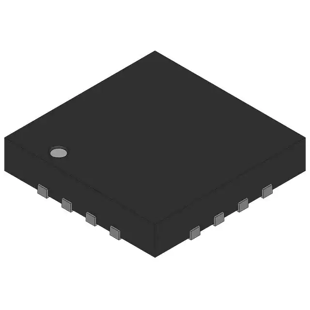
- Part No.:
- MMA5212AKW
- Manufacturer:
- NXP Semiconductors
- Category:
- Accelerometers
- Package:
- 16-QFN Exposed Pad
- Datasheet:
-
 MMA5212AKW.pdf
- Description:
- ACCELEROMETER 120G SPI 16QFN
- Quantity:
- Payment:

- Shipping:

Inventory:1,681
Please send an inquiry. Send us your inquiry, and we will respond immediately.
Product details
Overview
MMA5212AKW from NXP Semiconductors (formerly Freescale) is an X-axis satellite accelerometer engineered for PSI5 asynchronous mode automotive crash detection systems. It delivers ±120g full-scale range, 400 Hz 3-pole low-pass filtering, 16 μs internal sampling with 1 μs interpolation, PSI5 v1.3 compliance at 125 kBaud, and AEC-Q100 Grade 1 qualification (-40°C to +125°C). It operates in airbag front/side crash sensing applications where high-g overload immunity and EMC-robust power regulation are critical.
For engineers reviewing the MMA5212AKW datasheet, MMA5212AKW pinout, MMA5212AKW application, or MMA5212AKW equivalent, this page provides verified technical context, exact pin functions, real-world use scenarios in occupant safety systems, and validated alternative options for PSI5-based inertial sensing designs requiring ±120g range and AEC-Q100 compliance.
Technical Context
The MMA5212AKW implements an overdamped g-cell transducer with natural frequency of 12.65 kHz and damping ratio of 2.76, paired with a ΣΔ modulator feeding a 3rd-order sinc decimation filter (16:1 decimation), followed by configurable DSP stages including a fixed 400 Hz low-pass filter and selectable high-pass filters (0.04/0.1/0.3 Hz). Its PSI5 interface uses current modulation on IDATA with VCC powering both supply and data line via external resistor.
Internal voltage regulation employs three independent rails-VBUF (buffer regulator), VREG (digital supply), and VREGA (analog supply)-each monitored for undervoltage reset and capacitor presence. The device supports factory-programmed OTP configuration, serial number traceability, and built-in self-test with programmable repetition count and offset cancellation initialization sequence.
Key Specifications
| Parameter | Value and Actual Design Meaning |
|---|---|
| Full-Scale Range | ±120g - defines maximum measurable acceleration before clipping; matches front/side crash pulse profiles. |
| PSI5 Interface | v1.3 Asynchronous Mode, 125 kBaud - enables deterministic timing-critical communication over single-wire bus with even parity error detection. |
| Low-Pass Filter | 400 Hz, 3-pole - suppresses high-frequency noise while preserving crash event rise time integrity. |
| Sampling & Interpolation | 16 μs internal sample rate, interpolated to 1 μs resolution - supports precise timing alignment of crash onset detection. |
| Operating Temperature | -40°C to +125°C (AEC-Q100 Grade 1) - ensures reliability under hood and cabin thermal extremes. |
| Supply Architecture | VCC-powered with VBUF/VREG/VREGA triple-regulated rails - isolates analog/digital domains and maintains operation during VCC micro-cuts. |
| Self-Test Output | 40 LSB (10-bit) at ±120g range - provides in-system functional verification without mechanical stimulus. |
Pinout & Package
Pb-free 16-pin QFN package (Case 2086-01, 6 mm × 6 mm, 0.5 mm pitch) with exposed thermal pad internally connected to VSS.
| Pin/Terminal | Circuit Role | Design Meaning |
|---|---|---|
| VCC | PSI5 Power & Data Line Supply | Supplies device via external resistor; powers internal regulators and enables PSI5 current modulation on IDATA. |
| IDATA | PSI5 Response Current Output | Modulates sink current onto VCC line for PSI5 data transmission; requires external pull-up resistor. |
| VBUF | Buffer Regulator Input | Feeds isolated VREG (digital) and VREGA (analog) supplies; provides EMC resilience and dropout immunity. |
| VREG / VREGA | Digital / Analog Supply Outputs | Stable 2.50 V outputs (±3.8%); require dedicated 1 μF ceramic capacitors to VSS/VSSA for regulation integrity. |
| VSS / VSSA | Digital / Analog Ground Returns | Separate ground paths prevent digital switching noise from corrupting analog sensor signal chain. |
| TEST / SCLK / DIN / DOUT / CS | SPI Test Interface | Factory/test-only pins; must be grounded or left unconnected in production; not used during PSI5 operation. |
Key Features
| Feature | Design Value |
|---|---|
| PSI5 v1.3 Asynchronous Mode Compliance | Enables drop-in integration into existing PSI5 safety networks without protocol translation or gateway overhead. |
| Triple Independent Voltage Regulation (VBUF/VREG/VREGA) | Prevents system-level failure during transient supply disturbances; each rail has dedicated undervoltage detection and capacitor monitoring. |
| Factory-Programmed Full-Scale Range | RNG[2:0] = 011 encodes ±120g range in DEVCFG1 register - eliminates runtime configuration errors and ensures calibration consistency. |
| Offset Cancellation with Programmable HPF | Configurable high-pass filter corner frequencies (0.04/0.1/0.3 Hz) enable drift compensation tailored to vehicle mounting location and thermal profile. |
| Integrated Self-Test with Repetition Control | ST_RPT register allows up to 5 self-test repetitions on failure before reporting Sensor Error Message - improves diagnostic confidence in safety-critical deployments. |
Applications
| Front Airbag Crash Detection | Side Impact Occupant Sensing |
|---|---|
Use Scenario: Detects rapid deceleration during frontal collision to trigger airbag deployment within ≤30 ms. IC Role / Device Role / Timing Role: X-axis satellite accelerometer providing primary crash pulse input to airbag control unit via PSI5 bus. Use Value: ±120g range captures typical front crash pulses (20–80g peak); 400 Hz LPF preserves rise time <1 ms while rejecting road noise. | Use Scenario: Monitors lateral acceleration during side-impact events to determine seat position, occupant presence, and deployment threshold. IC Role / Device Role / Timing Role: Dedicated X-axis inertial sensor mounted in B-pillar or door module, communicating over PSI5 to central safety controller. Use Value: AEC-Q100 Grade 1 rating ensures operation at cabin temperatures up to +125°C; 1 μs interpolation enables precise impact timing correlation. |
| Seat Belt Pretensioner Activation | Roll-Over Detection Support |
Use Scenario: Triggers pretensioner retraction upon detecting pre-crash braking or initial crash jerk. IC Role / Device Role / Timing Role: Secondary acceleration input feeding predictive algorithms in occupant restraint ECU. Use Value: Low-latency 16 μs sampling and fast-startup HPF allow response to sub-100 ms pre-crash events; SPI test pins support end-of-line calibration. | Use Scenario: Provides X-axis acceleration reference for roll-rate estimation when fused with gyro data in rollover mitigation systems. IC Role / Device Role / Timing Role: Satellite sensor augmenting IMU data with high-accuracy, low-drift X-axis measurement. Use Value: Digital offset after cancellation limited to ±1 LSB ensures stable baseline for long-duration tilt calculation; VSSA isolation minimizes common-mode noise coupling. |
Equivalent & Alternatives
The following parts are listed as comparable options for similar inertial sensing applications.
| Alternative Part | Technical Difference | Application Difference | Selection Advice |
|---|---|---|---|
| NXP MMA5224AKW | ±240g full-scale range; higher g-cell clipping limit (2065g); identical PSI5 interface and package. | Targeted at rear-impact or high-speed crash detection where higher dynamic range is required. | Select when system-level crash pulse modeling exceeds ±120g but retains same PCB layout and firmware interface. |
| Analog Devices ADXL312WBRMZ-RL | I²C/SPI digital output; ±1.5g to ±12g range; no PSI5 support; 32-lead LFCSP package. | Designed for non-safety-critical motion sensing (e.g., telematics, infotainment), not crash detection. | Only suitable for development prototyping or secondary non-safety functions; requires complete interface redesign and new qualification. |
Compared with MMA5212AKW, MMA5224AKW offers extended range for higher-energy crash scenarios while maintaining pin, protocol, and qualification compatibility; ADXL312WBRMZ-RL provides higher resolution at low g but lacks PSI5, AEC-Q100 Grade 1, and crash-specific signal conditioning-making it unsuitable as a direct replacement in airbag systems.
Availability
MMA5212AKW is available at Aetrix Electronics and suitable for automotive airbag control units, side-impact sensing modules, seat belt pretensioner ECUs, and rollover mitigation systems requiring stable component supply with full AEC-Q100 traceability and long-term lifecycle support.
Supply support for MMA5212AKW includes scheduled delivery planning, volume procurement assistance, BOM continuity management, traceable sourcing, and lifecycle availability coordination for OEM customers, industrial embedded developers, connected-device designers, and electronics production programs.
Manufacturer
NXP Semiconductors is a global semiconductor leader focused on secure connectivity solutions for automotive, industrial, and IoT applications, with deep expertise in automotive safety ICs.
The MMA52xxAKW product line was developed specifically for PSI5-based automotive occupant safety systems, delivering robust inertial sensing with integrated diagnostics, EMC-hardened power architecture, and AEC-Q100-compliant reliability for airbag and restraint control.
FAQ
What is the full-scale range of the MMA5212AKW and how is it configured?
The MMA5212AKW has a factory-programmed full-scale range of ±120g, encoded in the RNG[2:0] bits of the DEVCFG1 register as '011'. This value is permanently programmed during manufacturing and cannot be altered in-field. The range determines sensitivity (4 LSB/g), clipping limits (±500g g-cell stop), and ADC saturation points. No external configuration or software command changes this setting-the MMA5212AKW is a dedicated ±120g variant within the MMA52xxAKW family.
Does the MMA5212AKW support SPI communication in production systems?
No, the MMA5212AKW does not support SPI communication in production operation. Pins SCLK, DIN, DOUT, and CS are reserved exclusively for factory test and characterization. Per the datasheet, these pins must be grounded or left unconnected in final application circuits. All operational communication occurs exclusively via the PSI5 asynchronous interface on VCC and IDATA pins. SPI functionality is disabled after power-on reset and is not accessible during normal device operation.
How does the MMA5212AKW handle power supply disturbances such as VCC micro-cuts?
The MMA5212AKW handles VCC micro-cuts using its triple-regulator architecture and dedicated monitoring. When VCC drops below 3.4 V (with 0.1–0.4 V hysteresis), PSI5 transmissions terminate immediately but the device remains powered via stored charge on VBUF, VREG, and VREGA capacitors. Internal reset is asserted only if VBUF, VREG, or VREGA fall below their individual undervoltage thresholds (e.g., VBUF_UV_F = 2.95 V). Recovery occurs automatically upon next PSI5 sync pulse once VCC recovers above threshold-no host intervention required.
What is the purpose of the VBUF pin and how is it different from VCC?
VBUF is the input to the internal buffer regulator, which generates isolated VREG (digital) and VREGA (analog) supplies. Unlike VCC-which serves as both PSI5 power line and data return path-VBUF provides a clean, filtered, and EMC-immune source for sensitive analog/digital circuitry. VCC connects directly to the vehicle's 12 V battery (via external resistor), while VBUF is decoupled with a 1 μF capacitor and regulates down to ~3.8 V. This separation prevents VCC ripple and transients from corrupting sensor measurements or digital logic, fulfilling AEC-Q100 EMC requirements.
Can the MMA5212AKW be used without external passive components?
No, the MMA5212AKW requires mandatory external components for stable operation. These include: (1) 1 μF ceramic capacitors on VREG–VSS, VREGA–VSSA, and VBUF–VSS (per Figure 1); (2) 2.2 nF and 15 nF decoupling caps on VCC; (3) 470 pF filter cap on IDATA; (4) 82 Ω resistor between VCC and vehicle power; and (5) 27 Ω resistor on IDATA. Omitting any of these violates the design validation conditions in the datasheet and risks undervoltage resets, signal corruption, or failure to meet AEC-Q100 EMC/thermal specs.
MMA5212AKW Specifications
- Product attributes
- Attribute value
- Manufacturer:
- NXP Semiconductors
- Series:
- MMA
- Package/Case:
- 16-QFN Exposed Pad
- Packaging:
- Tube
- Product Status:
- Not For New Designs
- Type:
- Digital
- Axis:
- X
- Acceleration Range:
- ±120g
- Sensitivity (LSB/g):
- 4
- Sensitivity (mV/g):
- -
- Bandwidth:
- -
- Output Type:
- SPI
- Voltage - Supply:
- 4.2V ~ 17V
- Features:
- -
- Operating Temperature:
- -40°C ~ 125°C
- Grade:
- Automotive
- Qualification:
- AEC-Q100
- Mounting Type:
- Surface Mount
- Supplier Device Package:
- 16-QFN (6x6)
MMA5212AKW FAQ
1.How can I place an order for MMA5212AKW through Aetrix?
Please submit a Request for Quotation (RFQ) for MMA5212AKW on Aetrix. Our sales agent will provide a competitive quotation and guide you through the order confirmation once you accept the terms.
2.Are the price and stock information for MMA5212AKW reliable?
The price and inventory of MMA5212AKW are updated periodically and may fluctuate due to market conditions. Stock and pricing data are typically refreshed every 24 hours. Quotation validity for MMA5212AKW is usually 5 days.
3.What payment methods are accepted for MMA5212AKW?
We accept Wire Transfer, PayPal, Credit Card, Western Union, MoneyGram, and Escrow for MMA5212AKW transactions.
Note: Certain payment methods may incur a processing fee.
4.How is shipping managed for MMA5212AKW?
MMA5212AKW orders can be shipped via leading logistics carriers, including DHL, UPS, FedEx, TNT, or Registered Mail.
Once your MMA5212AKW order is processed, you will receive an email with the shipment details and tracking number.
Note: Tracking information may take up to 24 hours to appear. Express delivery typically takes 3–5 business days.
5.How can I obtain technical support or documentation for MMA5212AKW?
For technical support, including MMA5212AKW datasheets, pinout diagrams, or application guidance, please contact our engineering support team. They can provide detailed documentation and assistance for your MMA5212AKW requirements.
6.How does Aetrix verify that MMA5212AKW is sourced from the original manufacturer or authorized distributors?
All MMA5212AKW products on Aetrix are procured from qualified distributors and authorized channels. Our dedicated quality assurance team conducts strict verification, including traceability checks and, if necessary, third-party testing. This ensures that MMA5212AKW meets industry standards.
7.What is the process for return or replacement of MMA5212AKW?
All MMA5212AKW units undergo pre-shipment inspection (PSI). If there is an issue with MMA5212AKW, returns or replacements are accepted under the following conditions:
1.Quantity discrepancies, incorrect items, or visible external defects (such as breakage or corrosion), acknowledged by Aetrix.
2.The issue is reported within 90 days of delivery.
3.The MMA5212AKW part is unused and in its original packaging.
Return procedure for MMA5212AKW:
1.Submit a request within 90 days.
2.Obtain a Return Material Authorization (RMA) from Aetrix.
MMA5212AKW Tags

-
MXC4005XC
Memsic Inc.

-
MC3419
Memsic Inc.

-
MC3479
Memsic Inc.

-
MXC6655XA
Memsic Inc.

-
MC3630
Memsic Inc.
.jpg)
-
LIS2HH12TR
STMicroelectronics

-
KX122-1037
Kionix Inc.
-
LIS2DE12TR
STMicroelectronics
-
LIS2DH12TR
STMicroelectronics

-
MC3635
Memsic Inc.
-
LIS2DS12TR
STMicroelectronics

-
LIS3DHTR
STMicroelectronics
Tech Hub

A practical engineering guide to 3.3V and 5V logic compatibility, input thresholds, resistor dividers, translator ICs, MOSFET level shifting, I2C pull-ups, timing limits and power-sequencing risks.

The 74HC595 uses push-pull logic outputs, while the TPIC6B595 uses 50 V open-drain DMOS sinks for higher-power loads. This guide compares timing, current limits, 3.3 V interfacing, load wiring, thermal…

The 74HC595 converts serial data into eight stable parallel outputs. This guide covers pin functions, shift and storage timing, OE and MR behavior, drive-current limits, cascading, voltage compatibilit…

A technical comparison of level-sensitive latches and edge-triggered flip-flops, covering timing windows, setup and hold limits, master–slave operation, time borrowing, race-through, HDL inference and…

A D latch stores one bit while Enable controls when data can pass. This reference covers gate-level operation, truth tables, transparency, setup and hold timing, LE versus OE, common ICs and practical …

An SR latch stores one bit through cross-coupled feedback. This engineering reference covers NOR and NAND implementations, truth tables, forbidden-state recovery, gated operation, switch debouncing, fa…

Latch circuits retain one bit through feedback. This technical reference covers SR and D latches, truth tables, transparency, timing limits, latch-versus-flip-flop behavior, applications and common log…

An engineering guide to LED driver operation, constant-current and constant-voltage outputs, linear and switching topologies, dimming, IC selection, calculations, replacement compatibility, and fault c…

Operational amplifier guide covering op amp basics, feedback, ideal vs real op amps, common configurations, buffer circuits, offset, bias current, gain-bandwidth, slew rate, rail-to-rail limits and sel…

Jumper cables guide covering safe connection order, red and black clamp placement, final ground connection, cable gauge, length, clamp quality, copper vs CCA cables, jump starter comparison and battery…


