
 My Inquiry
 My Account


NXP Semiconductors MMA6519KWR2
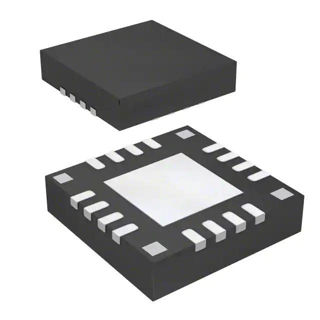
- Part No.:
- MMA6519KWR2
- Manufacturer:
- NXP Semiconductors
- Category:
- Accelerometers
- Package:
- 16-QFN Exposed Pad
- Datasheet:
-
 MMA6519KWR2.pdf
- Description:
- ACCELEROMETER 80G SPI 16QFN
- Quantity:
- Payment:

- Shipping:

Inventory:1,331
Please send an inquiry. Send us your inquiry, and we will respond immediately.
Product details
Overview
MMA6519KWR2 from NXP Semiconductors (formerly Freescale) is a dual-axis, SPI-interface, over-damped lateral accelerometer with ±80g full-scale range on both X and Y axes, 12-bit digital output, and AEC-Q100 Grade 1 qualification for automotive airbag deployment systems.
For engineers reviewing the MMA6519KWR2 datasheet, MMA6519KWR2 pinout, MMA6519KWR2 application, or MMA6519KWR2 equivalent, key selection criteria include its automotive-grade shock survivability (±2000g unpowered), programmable arming outputs per axis, twelve selectable low-pass filter options (50–1000 Hz), offset cancellation with <0.25 LSB/s slew rate, and Pb-free 16-pin QFN (6×6 mm) package.
Technical Context
The MMA6519KWR2 integrates two independent over-damped silicon MEMS g-cells with natural frequency of 10.8–15.9 kHz and damping ratio of 2.46–9.36, coupled to ΣΔ ADCs and configurable SINC/IIR digital filters. Its internal 8 MHz oscillator feeds programmable clock dividers to support DSP sample rates of 64/fOSC or 128/fOSC.
Each axis features independent register-controlled arming logic (open-drain ARM_X/ARM_Y), self-test activation with calibrated deflection values stored in OTP, and dual-mode offset correction-either automatic averaging (>6.29 s period) or manual register-based adjustment-with dedicated monitor thresholds (±100 LSB).
Key Specifications
| Parameter | Value and Actual Design Meaning |
|---|---|
| Full-Scale Range | ±80g on both X and Y axes - enables detection of high-deceleration crash events without saturation in front/side airbag triggers |
| Digital Output Resolution | 12-bit signed or unsigned SPI data - provides 4096 discrete levels for precise acceleration quantization |
| Supply Voltage | 3.3 V or 5.0 V single supply - supports legacy 5V automotive microcontrollers and modern 3.3V domain interfaces |
| Low-Pass Filter Options | 12 selectable cutoff frequencies (50–1000 Hz) - allows tuning noise rejection vs. response time for specific crash pulse profiles |
| Offset Cancellation Slew Rate | <0.25 LSB/s - prevents abrupt output shifts during thermal drift compensation, critical for stable arming decisions |
| AEC-Q100 Qualification | Grade 1 (−40°C to +105°C ambient) - validated for under-hood and passenger compartment deployment environments |
| Unpowered Shock Survivability | ±2000g (0.5 ms duration) - ensures mechanical integrity after severe pre-crash impacts before power-up |
Pinout & Package
Pb-free 16-pin QFN package, 6 mm × 6 mm, exposed die attach pad (internally connected to VSS), case number 2086-01.
| Pin/Terminal | Circuit Role | Design Meaning |
|---|---|---|
| VREGA | Analog supply input | Provides regulated 2.5 V for analog sensor front-end; requires 1 μF decoupling to VSSA |
| VSS, VSSA | Digital and analog ground | Separate return paths prevent digital switching noise from corrupting analog measurements |
| ARM_X / ARM_Y | Configurable arming output | Open-drain output per axis; programmable active-high/low for direct connection to airbag controller interrupt inputs |
| MISO / MOSI / SCLK / CS | SPI interface signals | Standard 4-wire SPI with internal pullup on CS and pulldowns on SCLK/MOSI - simplifies host-side termination |
| TEST/VPP | Factory programming voltage | Must be tied to VSS in application; not user-accessible during normal operation |
Key Features
| Feature | Design Value |
|---|---|
| Dual-axis independent arming | Each axis has dedicated ARM_X/ARM_Y output with configurable polarity and drive strength - enables axis-specific crash discrimination |
| Twelve programmable LPF settings | Four-pole and three-pole filter options from 50 Hz to 1000 Hz - matches filter response to vehicle-specific crash signature bandwidth |
| Self-test with factory-trimmed deflection | OTP-stored nominal ΔST values per axis (e.g., 582–872 LSB for ±80g range) - enables production-line functional verification without mechanical stimulus |
| Offset monitoring with threshold alert | ±100 LSB programmable thresholds on X/Y offset registers - triggers diagnostic flag if calibration drift exceeds safe limits |
| Over-damped MEMS sensing element | Damping ratio 2.46–9.36 and 10791–15879 Hz natural frequency - eliminates resonance-induced false triggers during high-frequency road vibration |
Applications
| Frontal Crash Detection | Side-Impact Sensing |
|---|---|
Use Scenario: Vehicle deceleration exceeding 30g within 20 ms during head-on collision. IC Role / Device Role / Timing Role: Dual-axis accelerometer providing real-time X/Y acceleration data to airbag control unit for deployment decision. Use Value: ±80g range and 400 Hz LPF option capture full crash pulse without clipping; <200 μs step response ensures sub-millisecond timing accuracy. | Use Scenario: Lateral acceleration >25g during T-bone impact at door pillar. IC Role / Device Role / Timing Role: Y-axis dominant sensing element feeding dedicated side-airbag trigger logic. Use Value: Independent Y-axis arming output (ARM_Y) asserts within 1.51 μs in unfiltered mode - meets ISO 26262 ASIL-B timing constraints. |
| Roll-Over Detection | Pre-Crash System Calibration |
Use Scenario: Vehicle angular rate and lateral acceleration indicating imminent rollover during high-speed turn. IC Role / Device Role / Timing Role: Y-axis acceleration measurement combined with yaw-rate sensor fusion input. Use Value: Cross-axis sensitivity <±4% ensures minimal X-axis interference during pure lateral maneuvers - improves roll-angle estimation fidelity. | Use Scenario: Continuous in-vehicle offset drift monitoring during ignition cycles. IC Role / Device Role / Timing Role: On-chip offset cancellation with >6.29 s averaging and real-time offset monitor. Use Value: <0.25 LSB/s slew rate prevents false alarms during thermal transients; ±100 LSB monitor threshold enables early warning of sensor degradation. |
Equivalent & Alternatives
The following parts are listed as comparable options for similar dual-axis automotive accelerometer applications.
| Alternative Part | Technical Difference | Application Difference | Selection Advice |
|---|---|---|---|
| MMA6525KWR2 | ±105g full-scale range per axis; identical pinout, interface, and package | Higher range suits heavy-vehicle or rollover-prone platforms requiring extended dynamic headroom | Select when crash pulse modeling predicts peak acceleration >80g but <105g |
| ADXL312WBRMZ-RL | 3-axis, 13-bit output, I²C/SPI interface; 3×4 mm LFCSP package; no AEC-Q100 Grade 1 certification | Lacks automotive qualification and dual-axis independent arming outputs - limited to non-safety-critical ADAS subsystems | Use only in non-safety applications where 3-axis data and smaller footprint outweigh qualification requirements |
Compared with MMA6525KWR2, the MMA6519KWR2 offers tighter offset stability and lower noise floor for 80g-range crash signatures; compared with ADXL312WBRMZ-RL, it delivers certified functional safety compliance and deterministic arming latency required for airbag ECU integration.
Availability
MMA6519KWR2 is available at Aetrix Electronics and suitable for automotive airbag control units, rollover detection modules, and pre-crash system calibration requiring stable component supply across long production lifecycles.
Supply support for MMA6519KWR2 includes scheduled delivery planning, volume procurement assistance, BOM continuity management, traceable sourcing, and lifecycle availability coordination for OEM customers, industrial embedded developers, connected-device designers, and electronics production programs.
Manufacturer
NXP Semiconductors is a global semiconductor company specializing in secure connectivity solutions for automotive, industrial, and IoT markets.
The MMA65xx family was designed specifically for automotive safety-critical inertial sensing, with emphasis on AEC-Q100 reliability, deterministic arming response, and integrated diagnostics for ASIL-B compliance in airbag deployment systems.
FAQ
What is the qualified operating temperature range for the MMA6519KWR2?
The MMA6519KWR2 is AEC-Q100 Grade 1 qualified, with a verified operating ambient temperature range of −40°C to +105°C. This range is confirmed by 100% final test and applies to all electrical characteristics including sensitivity, offset, and arming response time. The MMA6519KWR2 maintains full functionality across this range without derating.
Does the MMA6519KWR2 support both 3.3V and 5V supply voltages simultaneously?
No, the MMA6519KWR2 operates from a single supply voltage - either 3.3 V (±3.135–3.45 V) or 5.0 V (±4.75–5.25 V), selected at design time. VCC powers the digital core and SPI interface; VREG and VREGA are internally regulated to 2.5 V and must be decoupled externally. Mixing supplies is not supported and may damage the device.
How is the offset cancellation function configured and controlled in the MMA6519KWR2?
Offset cancellation in the MMA6519KWR2 is enabled via the OFFCFG_EN bit in DEVCTL register and controlled through DEVCFG register bits. It performs >6.29 s averaging with <0.25 LSB/s slew rate and updates correction every 1049 ms. The correction value (±0.25 LSB) and thresholds (±0.125 LSB) are fixed per design; no user scaling is required. The MMA6519KWR2 automatically applies correction to output data stream.
Can the ARM_X and ARM_Y pins of the MMA6519KWR2 be used as general-purpose digital outputs?
No - ARM_X and ARM_Y are dedicated arming outputs with configurable open-drain behavior (active-low/high) and pulldown/pullup current specs (50–100 μA). They cannot be reconfigured as generic GPIOs. Their assertion timing (≤1.51 μs in unfiltered mode) and fault-safe default state (high-impedance when disabled) are optimized exclusively for airbag ECU interrupt signaling.
What SPI timing parameters define the maximum achievable data rate for the MMA6519KWR2?
The MMA6519KWR2 supports SPI clock periods down to 120 ns (8.33 MHz max), with minimum high/low times of 40 ns each. Data setup (20 ns) and hold (10 ns) times constrain reliable communication. At 8 MHz, the device achieves ~1.25 MSps effective sampling rate before filtering. The MMA6519KWR2's tACCESS (60 ns) and tVALID (35 ns) ensure fast register read/write turnaround for real-time configuration.
MMA6519KWR2 Specifications
- Product attributes
- Attribute value
- Manufacturer:
- NXP Semiconductors
- Series:
- -
- Package/Case:
- 16-QFN Exposed Pad
- Packaging:
- Tape & Reel (TR)
- Product Status:
- Obsolete
- Type:
- Digital
- Axis:
- X, Y
- Acceleration Range:
- ±80g
- Sensitivity (LSB/g):
- 24
- Sensitivity (mV/g):
- -
- Bandwidth:
- -
- Output Type:
- SPI
- Voltage - Supply:
- 3.135V ~ 5.25V
- Features:
- Selectable Low Pass Filter
- Operating Temperature:
- -40°C ~ 105°C
- Grade:
- Automotive
- Qualification:
- AEC-Q100
- Mounting Type:
- Surface Mount
- Supplier Device Package:
- 16-QFN (6x6)
MMA6519KWR2 FAQ
1.How can I place an order for MMA6519KWR2 through Aetrix?
Please submit a Request for Quotation (RFQ) for MMA6519KWR2 on Aetrix. Our sales agent will provide a competitive quotation and guide you through the order confirmation once you accept the terms.
2.Are the price and stock information for MMA6519KWR2 reliable?
The price and inventory of MMA6519KWR2 are updated periodically and may fluctuate due to market conditions. Stock and pricing data are typically refreshed every 24 hours. Quotation validity for MMA6519KWR2 is usually 5 days.
3.What payment methods are accepted for MMA6519KWR2?
We accept Wire Transfer, PayPal, Credit Card, Western Union, MoneyGram, and Escrow for MMA6519KWR2 transactions.
Note: Certain payment methods may incur a processing fee.
4.How is shipping managed for MMA6519KWR2?
MMA6519KWR2 orders can be shipped via leading logistics carriers, including DHL, UPS, FedEx, TNT, or Registered Mail.
Once your MMA6519KWR2 order is processed, you will receive an email with the shipment details and tracking number.
Note: Tracking information may take up to 24 hours to appear. Express delivery typically takes 3–5 business days.
5.How can I obtain technical support or documentation for MMA6519KWR2?
For technical support, including MMA6519KWR2 datasheets, pinout diagrams, or application guidance, please contact our engineering support team. They can provide detailed documentation and assistance for your MMA6519KWR2 requirements.
6.How does Aetrix verify that MMA6519KWR2 is sourced from the original manufacturer or authorized distributors?
All MMA6519KWR2 products on Aetrix are procured from qualified distributors and authorized channels. Our dedicated quality assurance team conducts strict verification, including traceability checks and, if necessary, third-party testing. This ensures that MMA6519KWR2 meets industry standards.
7.What is the process for return or replacement of MMA6519KWR2?
All MMA6519KWR2 units undergo pre-shipment inspection (PSI). If there is an issue with MMA6519KWR2, returns or replacements are accepted under the following conditions:
1.Quantity discrepancies, incorrect items, or visible external defects (such as breakage or corrosion), acknowledged by Aetrix.
2.The issue is reported within 90 days of delivery.
3.The MMA6519KWR2 part is unused and in its original packaging.
Return procedure for MMA6519KWR2:
1.Submit a request within 90 days.
2.Obtain a Return Material Authorization (RMA) from Aetrix.
MMA6519KWR2 Tags

-
MXC4005XC
Memsic Inc.

-
MC3419
Memsic Inc.

-
MC3479
Memsic Inc.

-
MXC6655XA
Memsic Inc.

-
MC3630
Memsic Inc.
.jpg)
-
LIS2HH12TR
STMicroelectronics

-
KX122-1037
Kionix Inc.
-
LIS2DE12TR
STMicroelectronics
-
LIS2DH12TR
STMicroelectronics

-
MC3635
Memsic Inc.
-
LIS2DS12TR
STMicroelectronics

-
LIS3DHTR
STMicroelectronics
Tech Hub

A practical engineering guide to 3.3V and 5V logic compatibility, input thresholds, resistor dividers, translator ICs, MOSFET level shifting, I2C pull-ups, timing limits and power-sequencing risks.

The 74HC595 uses push-pull logic outputs, while the TPIC6B595 uses 50 V open-drain DMOS sinks for higher-power loads. This guide compares timing, current limits, 3.3 V interfacing, load wiring, thermal…

The 74HC595 converts serial data into eight stable parallel outputs. This guide covers pin functions, shift and storage timing, OE and MR behavior, drive-current limits, cascading, voltage compatibilit…

A technical comparison of level-sensitive latches and edge-triggered flip-flops, covering timing windows, setup and hold limits, master–slave operation, time borrowing, race-through, HDL inference and…

A D latch stores one bit while Enable controls when data can pass. This reference covers gate-level operation, truth tables, transparency, setup and hold timing, LE versus OE, common ICs and practical …

An SR latch stores one bit through cross-coupled feedback. This engineering reference covers NOR and NAND implementations, truth tables, forbidden-state recovery, gated operation, switch debouncing, fa…

Latch circuits retain one bit through feedback. This technical reference covers SR and D latches, truth tables, transparency, timing limits, latch-versus-flip-flop behavior, applications and common log…

An engineering guide to LED driver operation, constant-current and constant-voltage outputs, linear and switching topologies, dimming, IC selection, calculations, replacement compatibility, and fault c…

Operational amplifier guide covering op amp basics, feedback, ideal vs real op amps, common configurations, buffer circuits, offset, bias current, gain-bandwidth, slew rate, rail-to-rail limits and sel…

Jumper cables guide covering safe connection order, red and black clamp placement, final ground connection, cable gauge, length, clamp quality, copper vs CCA cables, jump starter comparison and battery…


