
 My Inquiry
 My Account


NXP Semiconductors MMA6555KCWR2
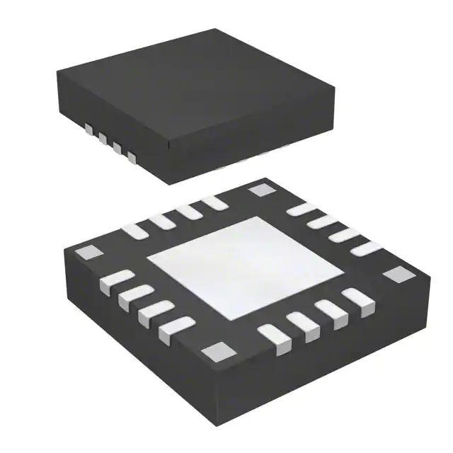
- Part No.:
- MMA6555KCWR2
- Manufacturer:
- NXP Semiconductors
- Category:
- Accelerometers
- Package:
- 16-QFN Exposed Pad
- Datasheet:
-
 MMA6555KCWR2.pdf
- Description:
- ACCELEROMETER 105G SPI 16QFN
- Quantity:
- Payment:

- Shipping:

Inventory:3,180
Please send an inquiry. Send us your inquiry, and we will respond immediately.
Product details
Overview
MMA6555KCWR2 from NXP Semiconductors is a single-axis, SPI-interface, over-damped lateral accelerometer with ±105 g full-scale range, 12-bit digital output, and AEC-Q100 Grade 1 qualification for automotive airbag systems. It operates from 3.3 V or 5 V supply, features twelve programmable low-pass filter options (50–1000 Hz), and integrates offset cancellation with < 0.25 LSB/s slew rate.
For engineers reviewing the MMA6555KCWR2 datasheet, MMA6555KCWR2 pinout, MMA6555KCWR2 application, or MMA6555KCWR2 equivalent, this page delivers verified technical context, real-world automotive timing and safety-critical interface constraints, package-validated thermal performance, and functional alternatives aligned to airbag control unit (ACU) design requirements.
Technical Context
The MMA6555KCWR2 implements a sigma-delta (ΣΔ) modulator with 1 MHz sampling, followed by configurable SINC and IIR low-pass filtering - supporting 12 distinct cutoff frequencies across two time-step modes (8 μs and 16 μs). Its internal analog front-end includes dedicated voltage regulators (VREG/VREGA), self-test circuitry, and offset monitoring with programmable thresholds (±100 LSB).
It uses an over-damped mechanical sensing element (damping ratio ζ = 2.46–9.36) with natural frequency 10.8–15.9 kHz and 0.85–2.29 kHz −3 dB cutoff, ensuring minimal phase distortion and robust response to crash-induced transients. The ARM/PCM pin supports configurable arming output or PCM data streaming, synchronized to SPI frame timing.
Key Specifications
| Parameter | Value and Actual Design Meaning |
|---|---|
| Full-Scale Range | ±105 g - calibrated for airbag deployment threshold detection without clipping up to 500 g mechanical input |
| Digital Output Resolution | 12-bit signed/unsigned SPI - provides 0.051 g/LSB sensitivity (18.2 LSB/g) for precise acceleration quantization |
| Supply Voltage | 3.3 V or 5.0 V single supply - compatible with standard automotive microcontroller I/O domains and regulator outputs |
| Low-Pass Filter Options | 12 selectable configurations (50–1000 Hz) - enables tuning for crash pulse discrimination vs. noise rejection in ACU algorithms |
| Offset Cancellation | 6.29 s averaging period, < 0.25 LSB/s slew rate - eliminates thermal drift while preserving dynamic response during pre-crash vehicle maneuvers |
| AEC-Q100 Qualification | Grade 1 (−40 °C to +105 °C) - validated for under-hood and passenger compartment mounting in production vehicles |
| Package | Pb-free 16-pin QFN, 6 mm × 6 mm × 1.98 mm - surface-mount compatible with automated reflow and meets automotive thermal dissipation requirements (θJC = 2.5 °C/W) |
Pinout & Package
Pb-free 16-pin QFN package (6 mm × 6 mm × 1.98 mm) with exposed die attach pad internally connected to VSS. Pin 17 (PAD) and corner pads are electrically tied to digital ground for thermal and EMI performance.
| Pin/Terminal | Circuit Role | Design Meaning |
|---|---|---|
| VREGA | Analog supply input | Provides regulated power to analog signal chain; requires 1 μF X7R capacitor to VSSA per layout guidelines |
| VSS / VSSA | Digital and analog ground | Separate return paths prevent digital switching noise from corrupting sensor ADC conversion |
| VCC | Main supply input | Accepts 3.3 V or 5 V; internal undervoltage monitor asserts reset if drops below 2.74 V (3.3 V mode) |
| CS, SCLK, MOSI, MISO | SPI interface signals | Standard 4-wire SPI with 8 MHz internal clock; tACCESS ≤ 60 ns ensures timing margin for 10 MHz MCU interfaces |
| ARM/PCM | Configurable output | Programmable as open-drain arming flag (for ACU wake-up) or PCM data stream proportional to acceleration |
| TEST/VPP | Factory programming voltage | Must be tied to VSS in application; not user-accessible during normal operation |
Key Features
| Feature | Design Value |
|---|---|
| Over-damped lateral sensing element | Eliminates resonance-induced false triggers during high-frequency road noise or engine vibration |
| Programmable arming function | Enables hardware-level event latching for crash detection, reducing software polling overhead in safety-critical ACUs |
| Self-test with factory-trimmed deflection value | Allows in-system verification of MEMS functionality and signal chain integrity without external stimulus |
| Offset monitor with ±100 LSB thresholds | Flags excessive zero-g drift before it compromises crash detection accuracy, supporting ISO 26262 diagnostic coverage |
| Internal voltage regulators (VREG/VREGA) | Isolates digital and analog domains, enabling stable operation despite battery ripple or load dump conditions |
Applications
| Frontal Crash Detection | Side-Impact Sensing |
|---|---|
Use Scenario: Mounted on vehicle firewall or tunnel to detect rapid deceleration during head-on collisions. IC Role / Device Role / Timing Role: Primary acceleration transducer feeding real-time data to airbag control unit (ACU) for deployment decision within 10–30 ms. Use Value: ±105 g range and 400 Hz LPF option capture crash pulse shape with < 100 μs group delay, meeting FMVSS 208 timing requirements. | Use Scenario: Integrated into door modules or B-pillars to sense lateral acceleration during T-bone impacts. IC Role / Device Role / Timing Role: Single-axis lateral sensor providing directional crash vector to ACU for side airbag and curtain deployment logic. Use Value: Over-damped mechanical response rejects door slam artifacts, while AEC-Q100 Grade 1 ensures reliability at cabin temperatures up to +105 °C. |
| Roll-Over Detection | Pre-Crash System Input |
Use Scenario: Mounted near vehicle center of gravity to monitor angular acceleration during rollover events. IC Role / Device Role / Timing Role: Lateral axis input to rollover algorithm, used alongside yaw rate and steering angle for early warning activation. Use Value: 50 Hz LPF mode suppresses high-frequency suspension noise while preserving slow-roll dynamics for accurate tilt estimation. | Use Scenario: Embedded in ADAS domain controller to feed acceleration history into predictive collision avoidance models. IC Role / Device Role / Timing Role: Safety-relevant sensor supplying longitudinal/lateral jerk data for braking and steering intervention timing. Use Value: Offset cancellation and 12-bit resolution enable sub-0.1 g measurement stability over temperature, critical for pre-crash trajectory prediction. |
Equivalent & Alternatives
The following parts are listed as comparable options for similar single-axis automotive accelerometer applications.
| Alternative Part | Technical Difference | Application Difference | Selection Advice |
|---|---|---|---|
| ADXL372WBCPZ-RL7 | 200 g range, 2.5 V supply only, I²C/SPI interface, lower current (19 μA standby) | Targeted at ultra-low-power event-triggered wake-up; lacks AEC-Q100 Grade 1 rating | Select for battery-powered telematics or secondary crash sensors where extended temperature range is not required |
| MMA6556KCWR2 | Identical package and pinout; ±120 g full-scale range, 16.0 LSB/g sensitivity | Higher range suits rear-impact or heavy-vehicle applications; same AEC-Q100 Grade 1 qualification | Drop-in replacement when system-level crash pulse modeling requires extended headroom beyond ±105 g |
Compared with ADXL372WBCPZ-RL7, MMA6555KCWR2 offers guaranteed automotive qualification and higher supply flexibility; compared with MMA6556KCWR2, it trades 15 g range for improved LSB/g resolution and lower noise floor in 400 Hz LPF mode - optimizing for frontal crash pulse fidelity.
Availability
MMA6555KCWR2 is available at Aetrix Electronics and suitable for automotive airbag control units, rollover detection systems, and pre-crash ADAS modules requiring stable component supply, AEC-Q100-compliant traceability, and tape-and-reel packaging for high-volume SMT assembly.
Supply support for MMA6555KCWR2 includes scheduled delivery planning, volume procurement assistance, BOM continuity management, traceable sourcing, and lifecycle availability coordination for OEM customers, industrial embedded developers, connected-device designers, and electronics production programs.
Manufacturer
NXP Semiconductors is a global semiconductor leader focused on secure connectivity solutions for automotive, industrial, and IoT applications, with deep expertise in safety-critical sensor and microcontroller design.
The MMA655x family is part of NXP's SafeAssure portfolio - engineered specifically for ASIL-B compliant automotive safety systems, emphasizing functional safety, diagnostic coverage, and long-term reliability in harsh vehicular environments.
FAQ
What is the operating temperature range qualified for the MMA6555KCWR2?
The MMA6555KCWR2 is AEC-Q100 Grade 1 qualified, with a verified operating ambient temperature range of −40 °C to +105 °C. This range is confirmed by 100% final test and applies to all electrical characteristics including sensitivity, offset, and SPI timing parameters - making it suitable for under-hood and passenger compartment deployments where thermal cycling is severe.
Does the MMA6555KCWR2 support both 3.3 V and 5 V supply voltages simultaneously?
No - the MMA6555KCWR2 operates from a single supply voltage: either 3.3 V (±3.135 V to ±3.45 V) or 5.0 V (±4.75 V to ±5.25 V), selected at system level. VREG and VREGA regulators derive internal rails from VCC; mixing supplies is not supported and would violate absolute maximum ratings for VREG (−0.3 V to +3.0 V).
How is the ARM pin configured for arming output versus PCM output in the MMA6555KCWR2?
The ARM/PCM pin function is set via the DEVCFG register (address $0B, bit A_CFG[2:0]). Writing A_CFG = 000 configures it as an open-drain arming output (active-low or active-high, programmable); writing A_CFG = 001 selects PCM output mode. Configuration must occur before ENDINIT is set, and the pin defaults to high-impedance if unused - no external pull-up is required unless arming mode is enabled.
What low-pass filter options are available on the MMA6555KCWR2 and how are they selected?
The MMA6555KCWR2 offers twelve low-pass filter options: six at 8 μs timing (100–1000 Hz) and six at 16 μs timing (50–500 Hz), selected via LPF[3:0] bits in AXISCFG register ($0C). Each option uses a configurable IIR architecture; cutoff frequencies are −3 dB referenced to 0 Hz response, and filter group delay is explicitly characterized (e.g., 2.50 ms for 400 Hz 4-pole mode).
Is the MMA6555KCWR2 pin-compatible with other devices in the MMA655x family?
Yes - all MMA655x variants (including MMA6555KCWR2, MMA6556KCWR2, MMA6555KCW, and MMA6556KCW) share identical 16-pin QFN package (98ASA00690D), pinout, and footprint. Differences are limited to full-scale range (±105 g vs. ±120 g) and ordering format (tape-and-reel vs. tube); no PCB redesign is needed when substituting within the same range grade.
MMA6555KCWR2 Specifications
- Product attributes
- Attribute value
- Manufacturer:
- NXP Semiconductors
- Series:
- MMA
- Package/Case:
- 16-QFN Exposed Pad
- Packaging:
- Tape & Reel (TR)
- Product Status:
- Obsolete
- Type:
- Digital
- Axis:
- X
- Acceleration Range:
- ±105g
- Sensitivity (LSB/g):
- 18.2
- Sensitivity (mV/g):
- -
- Bandwidth:
- -
- Output Type:
- SPI
- Voltage - Supply:
- 3.135V ~ 5.25V
- Features:
- Selectable Low Pass Filter
- Operating Temperature:
- -40°C ~ 105°C
- Grade:
- Automotive
- Qualification:
- AEC-Q100
- Mounting Type:
- Surface Mount
- Supplier Device Package:
- 16-QFN (6x6)
MMA6555KCWR2 FAQ
1.How can I place an order for MMA6555KCWR2 through Aetrix?
Please submit a Request for Quotation (RFQ) for MMA6555KCWR2 on Aetrix. Our sales agent will provide a competitive quotation and guide you through the order confirmation once you accept the terms.
2.Are the price and stock information for MMA6555KCWR2 reliable?
The price and inventory of MMA6555KCWR2 are updated periodically and may fluctuate due to market conditions. Stock and pricing data are typically refreshed every 24 hours. Quotation validity for MMA6555KCWR2 is usually 5 days.
3.What payment methods are accepted for MMA6555KCWR2?
We accept Wire Transfer, PayPal, Credit Card, Western Union, MoneyGram, and Escrow for MMA6555KCWR2 transactions.
Note: Certain payment methods may incur a processing fee.
4.How is shipping managed for MMA6555KCWR2?
MMA6555KCWR2 orders can be shipped via leading logistics carriers, including DHL, UPS, FedEx, TNT, or Registered Mail.
Once your MMA6555KCWR2 order is processed, you will receive an email with the shipment details and tracking number.
Note: Tracking information may take up to 24 hours to appear. Express delivery typically takes 3–5 business days.
5.How can I obtain technical support or documentation for MMA6555KCWR2?
For technical support, including MMA6555KCWR2 datasheets, pinout diagrams, or application guidance, please contact our engineering support team. They can provide detailed documentation and assistance for your MMA6555KCWR2 requirements.
6.How does Aetrix verify that MMA6555KCWR2 is sourced from the original manufacturer or authorized distributors?
All MMA6555KCWR2 products on Aetrix are procured from qualified distributors and authorized channels. Our dedicated quality assurance team conducts strict verification, including traceability checks and, if necessary, third-party testing. This ensures that MMA6555KCWR2 meets industry standards.
7.What is the process for return or replacement of MMA6555KCWR2?
All MMA6555KCWR2 units undergo pre-shipment inspection (PSI). If there is an issue with MMA6555KCWR2, returns or replacements are accepted under the following conditions:
1.Quantity discrepancies, incorrect items, or visible external defects (such as breakage or corrosion), acknowledged by Aetrix.
2.The issue is reported within 90 days of delivery.
3.The MMA6555KCWR2 part is unused and in its original packaging.
Return procedure for MMA6555KCWR2:
1.Submit a request within 90 days.
2.Obtain a Return Material Authorization (RMA) from Aetrix.
MMA6555KCWR2 Tags

-
MXC4005XC
Memsic Inc.

-
MC3419
Memsic Inc.

-
MC3479
Memsic Inc.

-
MXC6655XA
Memsic Inc.

-
MC3630
Memsic Inc.
.jpg)
-
LIS2HH12TR
STMicroelectronics

-
KX122-1037
Kionix Inc.
-
LIS2DE12TR
STMicroelectronics
-
LIS2DH12TR
STMicroelectronics

-
MC3635
Memsic Inc.
-
LIS2DS12TR
STMicroelectronics

-
LIS3DHTR
STMicroelectronics
Tech Hub

A practical engineering guide to 3.3V and 5V logic compatibility, input thresholds, resistor dividers, translator ICs, MOSFET level shifting, I2C pull-ups, timing limits and power-sequencing risks.

The 74HC595 uses push-pull logic outputs, while the TPIC6B595 uses 50 V open-drain DMOS sinks for higher-power loads. This guide compares timing, current limits, 3.3 V interfacing, load wiring, thermal…

The 74HC595 converts serial data into eight stable parallel outputs. This guide covers pin functions, shift and storage timing, OE and MR behavior, drive-current limits, cascading, voltage compatibilit…

A technical comparison of level-sensitive latches and edge-triggered flip-flops, covering timing windows, setup and hold limits, master–slave operation, time borrowing, race-through, HDL inference and…

A D latch stores one bit while Enable controls when data can pass. This reference covers gate-level operation, truth tables, transparency, setup and hold timing, LE versus OE, common ICs and practical …

An SR latch stores one bit through cross-coupled feedback. This engineering reference covers NOR and NAND implementations, truth tables, forbidden-state recovery, gated operation, switch debouncing, fa…

Latch circuits retain one bit through feedback. This technical reference covers SR and D latches, truth tables, transparency, timing limits, latch-versus-flip-flop behavior, applications and common log…

An engineering guide to LED driver operation, constant-current and constant-voltage outputs, linear and switching topologies, dimming, IC selection, calculations, replacement compatibility, and fault c…

Operational amplifier guide covering op amp basics, feedback, ideal vs real op amps, common configurations, buffer circuits, offset, bias current, gain-bandwidth, slew rate, rail-to-rail limits and sel…

Jumper cables guide covering safe connection order, red and black clamp placement, final ground connection, cable gauge, length, clamp quality, copper vs CCA cables, jump starter comparison and battery…


