
 My Inquiry
 My Account


NXP Semiconductors MMA7341LCT
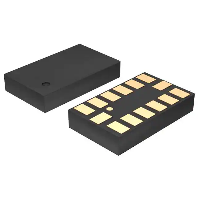
- Part No.:
- MMA7341LCT
- Manufacturer:
- NXP Semiconductors
- Category:
- Accelerometers
- Package:
- 14-TFLGA
- Datasheet:
-
 MMA7341LCT.pdf
- Description:
- ACCELEROMETER 3-9G ANALOG 14LGA
- Quantity:
- Payment:

- Shipping:

Inventory:3,943
Please send an inquiry. Send us your inquiry, and we will respond immediately.
Product details
Overview
MMA7341LCT from Freescale Semiconductor is a 3-axis capacitive MEMS accelerometer with integrated signal conditioning, selectable ±3g/±9g ranges, 400 μA active current, and Sleep Mode (3 μA). It delivers ratiometric analog outputs (XOUT/YOUT/ZOUT), features self-test and g-Select logic control, and targets battery-powered motion sensing in handheld electronics.
For engineers reviewing the MMA7341LCT datasheet, MMA7341LCT pinout, MMA7341LCT application, or MMA7341LCT equivalent, key selection criteria include its LGA-14 package footprint, 0.5 ms enable response time, ±5000g shock survivability, and compatibility with 2.2–3.6 V supply rails in space-constrained portable designs.
Technical Context
The MMA7341LCT integrates a surface-micromachined polysilicon g-cell sensor with an ASIC implementing switched-capacitor C-to-V conversion, 1-pole low-pass filtering, temperature compensation, and NVM-trimmed offset/sensitivity calibration. Its output voltage is ratiometric to VDD, enabling direct interface with microcontroller ADCs without external reference.
Control logic responds to digital inputs on Sleep (pin 7), g-Select (pin 10), and Self Test (pin 13) to dynamically configure operating mode, full-scale range, and mechanical integrity verification. The internal 11 kHz sampling clock drives the switched-capacitor filter, with output bandwidths of 400 Hz (XY) and 300 Hz (Z) under recommended 3.3 nF external filtering.
Key Specifications
| Parameter | Value and Actual Design Meaning |
|---|---|
| Supply Voltage | 2.2 V to 3.6 V - supports single-cell Li-ion and dual-cell alkaline systems without regulation |
| Active Current | 400 μA typ - enables >1-year operation on 200 mAh coin cell in periodic wake-up mode |
| Sleep Current | 3 μA typ - reduces power by 133× for ultra-low-duty-cycle motion-triggered wakeups |
| Sensitivity Options | ±3g @ 440 mV/g or ±9g @ 117.8 mV/g - selected via logic level on g-Select pin, no external components needed |
| Zero-g Output | 1.65 V at VDD = 3.3 V - centered at midsupply for symmetric positive/negative acceleration detection |
| Enable Response Time | 0.5 ms - allows rapid transition from sleep to valid output for event-driven applications like freefall detection |
| Shock Survivability | ±5000 g - withstands mechanical stress during drop testing and handling without calibration shift |
Pinout & Package
Package: 3 mm × 5 mm × 1.0 mm LGA-14 (Case 1977-01), bottom-terminal land grid array with exposed thermal pad (not electrically connected).
| Pin/Terminal | Circuit Role | Design Meaning |
|---|---|---|
| 1, 8, 9, 11, 12, 14 | No Connect | Internally unconnected; must remain floating per datasheet - no pull-up/down or routing required |
| 2 (XOUT) | Analog Output | Ratiometric voltage proportional to X-axis acceleration; requires 3.3 nF capacitor to suppress switched-capacitor clock noise |
| 3 (ZOUT) | Analog Output | Ratiometric voltage proportional to Z-axis acceleration; shares same signal chain architecture and bandwidth as XOUT/YOUT |
| 4 (YOUT) | Analog Output | Ratiometric voltage proportional to Y-axis acceleration; output impedance 32 kΩ necessitates ≥10 MΩ input impedance for minimal loading error |
| 5 (VSS) | Ground Reference | Primary analog ground return; must be tied directly to low-impedance PCB ground plane beneath device |
| 6 (VDD) | Power Input | 2.2–3.6 V supply; requires 0.1 μF ceramic decoupling capacitor placed within 2 mm of pin |
| 7 (Sleep) | Digital Control Input | Active-low enable: low = Sleep Mode (3 μA), high = active operation; internal pull-up not provided |
| 10 (g-Select) | Digital Control Input | Logic level selects full-scale range: low = ±3g (440 mV/g), high = ±9g (117.8 mV/g); internal pull-down defaults to 3g if left open |
| 13 (Self Test) | Digital Control Input | Pulse-high initiates electrostatic self-test: deflects X/Y axes slightly, Z axis by ~1g for functional verification pre-deployment |
Key Features
| Feature | Design Value |
|---|---|
| Ratiometric Output | Output offset and sensitivity scale linearly with VDD - eliminates need for external voltage reference when interfacing with MCU ADCs |
| Integrated Low-Pass Filter | On-chip switched-capacitor 1-pole filter - sets bandwidth to 400 Hz (XY) / 300 Hz (Z) without external RC components |
| Factory-Calibrated Offset & Sensitivity | Zero-g offset and gain trimmed in production - no external calibration components or firmware compensation required |
| Temperature Compensation | X/Y/Z offset drift ≤ ±2 mg/°C and sensitivity drift ≤ ±0.0075 %/°C - maintains accuracy across -40°C to +85°C industrial range |
| Robust Mechanical Design | Hermetically sealed wafer-level packaging - ensures long-term stability and immunity to humidity and particulate contamination |
Applications
| Laptop Freefall Protection | HDD MP3 Player Drop Detection |
|---|---|
Use Scenario: Detecting sudden vertical acceleration loss during laptop drop to park HDD heads before impact. IC Role / Device Role / Timing Role: Analog 3-axis motion sensor providing real-time acceleration data to system controller for predictive head retraction. Use Value: Enables <10 ms reaction window using 0.5 ms enable time and 400 Hz XY bandwidth to trigger mechanical protection before physical impact. | Use Scenario: Identifying uncontrolled descent in portable audio players to disable write operations and prevent storage corruption. IC Role / Device Role / Timing Role: Low-power motion monitor that wakes host processor only upon sustained negative-Z acceleration exceeding threshold. Use Value: Achieves multi-month standby via 3 μA Sleep Mode current while maintaining sub-100 ms detection latency for reliable drop capture. |
| Mobile Phone Motion UI | Pedometer Step Counting |
Use Scenario: Enabling tilt-based text scrolling, motion dialing, and eCompass tilt compensation in smartphones. IC Role / Device Role / Timing Role: Primary orientation sensor feeding real-time XYZ analog outputs to application processor for gesture recognition algorithms. Use Value: Delivers ±3g/±9g range selectability to optimize resolution for fine gestures (3g) or coarse motion (9g) without hardware change. | Use Scenario: Capturing vertical hip acceleration peaks during walking/running to calculate step count and distance. IC Role / Device Role / Timing Role: Low-noise analog front-end converting biomechanical motion into conditioned voltage waveforms for digital processing. Use Value: Provides 350 μg/√Hz noise density and factory-trimmed nonlinearity (<±1% FSO) to support accurate stride detection at sub-0.1g thresholds. |
Equivalent & Alternatives
The following parts are listed as comparable options for similar 3-axis analog-output MEMS accelerometer applications.
| Alternative Part | Technical Difference | Application Difference | Selection Advice |
|---|---|---|---|
| ADXL335BCPZ | Wider supply range (1.8–3.6 V), higher noise (500 μg/√Hz), no Sleep Mode, fixed ±3g range | Lacks dynamic range switching and ultra-low-power sleep - unsuitable for battery-critical drop-detection use cases | Select ADXL335BCPZ only when broader supply tolerance and legacy design continuity outweigh power and flexibility requirements. |
| KXSC7-2050 | Lower active current (120 μA), I²C digital output, built-in FIFO, ±2g/±4g/±8g programmable ranges | Requires digital interface and firmware driver stack - adds complexity versus MMA7341LCT's direct analog ADC connection | Choose KXSC7-2050 when system already uses I²C peripherals and benefits from on-chip data buffering and configurable ODR. |
Compared with ADXL335BCPZ and KXSC7-2050, the MMA7341LCT uniquely balances analog simplicity, dual-range flexibility, and sub-5 μA sleep power - making it optimal for cost-sensitive, space-constrained portable devices needing immediate wake-on-motion without digital protocol overhead.
Availability
MMA7341LCT is available at Aetrix Electronics and suitable for laptop freefall protection, mobile phone motion UI, and pedometer step counting requiring stable component supply and long-term industrial-grade availability.
Supply support for MMA7341LCT includes scheduled delivery planning, volume procurement assistance, BOM continuity management, traceable sourcing, and lifecycle availability coordination for OEM customers, industrial embedded developers, connected-device designers, and electronics production programs.
Manufacturer
Freescale Semiconductor (now part of NXP Semiconductors) is a global semiconductor company specializing in embedded processing, sensors, and connectivity solutions for automotive, industrial, and consumer markets.
The MMA7341LCT belongs to Freescale's Xtrinsic™ family of intelligent sensors, designed specifically for ultra-low-power motion awareness in portable electronics where size, battery life, and analog integration are critical constraints.
FAQ
What is the supply voltage range supported by the MMA7341LCT?
The MMA7341LCT operates from 2.2 V to 3.6 V DC. Within this range, it maintains full calibration and specified performance including offset, sensitivity, and bandwidth. Operation below 2.2 V or above 3.6 V may result in undefined behavior or permanent damage, as confirmed by the Absolute Maximum Ratings table in the official datasheet. The MMA7341LCT's ratiometric output ensures consistent scaling across this entire voltage window without external reference components.
How does the g-Select pin configure the MMA7341LCT's measurement range?
The g-Select pin (pin 10) is a logic input that selects between ±3g (440 mV/g) and ±9g (117.8 mV/g) full-scale ranges. A low logic level configures ±3g for high-resolution motion detection, while a high level selects ±9g for wider dynamic range. If left unconnected, the internal pull-down defaults the MMA7341LCT to ±3g mode. This configuration is active immediately upon power-up and can be changed dynamically during operation without reset.
What is the purpose of the Sleep pin on the MMA7341LCT, and how is it used?
The Sleep pin (pin 7) is an active-low digital control input that places the MMA7341LCT into ultra-low-power Sleep Mode (3 μA typical) when driven low, disabling all analog outputs. Driving it high resumes normal operation with 400 μA typical current draw and valid outputs within 0.5 ms. No internal pull-up exists, so external logic or MCU GPIO must actively drive the pin. This feature enables duty-cycled operation in battery-powered devices such as pedometers and mobile phones using the MMA7341LCT.
Can the MMA7341LCT be used without external filtering components?
The MMA7341LCT requires external 3.3 nF capacitors on each analog output (XOUT/YOUT/ZOUT) to suppress switched-capacitor clock noise, as specified in the datasheet's "Basic Connections" section. While the internal filter sets bandwidth, omitting these capacitors results in measurable 11 kHz ripple on outputs, degrading ADC accuracy. A 0.1 μF capacitor on VDD is also mandatory for power rail decoupling. Therefore, the MMA7341LCT cannot be used reliably without these two external components per the validated reference design.
What is the maximum mechanical shock the MMA7341LCT can survive without damage?
The MMA7341LCT is rated for ±5000 g mechanical shock across all axes, as defined in the Absolute Maximum Ratings table. This specification reflects survivability during handling, drop testing (e.g., 1.8 m onto concrete), and board-level reflow - not operational measurement range. The device maintains calibration integrity after such events due to its hermetically sealed wafer-level packaging and robust polysilicon g-cell structure, ensuring long-term reliability in rugged portable applications using the MMA7341LCT.
MMA7341LCT Specifications
- Product attributes
- Attribute value
- Manufacturer:
- NXP Semiconductors
- Series:
- -
- Package/Case:
- 14-TFLGA
- Packaging:
- Tray
- Product Status:
- Obsolete
- Type:
- Analog
- Axis:
- X, Y, Z
- Acceleration Range:
- ±3g, 9g
- Sensitivity (LSB/g):
- -
- Sensitivity (mV/g):
- 440 (±3g) ~ 117.8 (±9g)
- Bandwidth:
- 400Hz (X,Y), 300Hz (Z)
- Output Type:
- Analog Voltage
- Voltage - Supply:
- 2.2V ~ 3.6V
- Features:
- Selectable Scale, Sleep Mode
- Operating Temperature:
- -40°C ~ 85°C
- Grade:
- -
- Qualification:
- -
- Mounting Type:
- Surface Mount
- Supplier Device Package:
- 14-LGA (3x5)
MMA7341LCT FAQ
1.How can I place an order for MMA7341LCT through Aetrix?
Please submit a Request for Quotation (RFQ) for MMA7341LCT on Aetrix. Our sales agent will provide a competitive quotation and guide you through the order confirmation once you accept the terms.
2.Are the price and stock information for MMA7341LCT reliable?
The price and inventory of MMA7341LCT are updated periodically and may fluctuate due to market conditions. Stock and pricing data are typically refreshed every 24 hours. Quotation validity for MMA7341LCT is usually 5 days.
3.What payment methods are accepted for MMA7341LCT?
We accept Wire Transfer, PayPal, Credit Card, Western Union, MoneyGram, and Escrow for MMA7341LCT transactions.
Note: Certain payment methods may incur a processing fee.
4.How is shipping managed for MMA7341LCT?
MMA7341LCT orders can be shipped via leading logistics carriers, including DHL, UPS, FedEx, TNT, or Registered Mail.
Once your MMA7341LCT order is processed, you will receive an email with the shipment details and tracking number.
Note: Tracking information may take up to 24 hours to appear. Express delivery typically takes 3–5 business days.
5.How can I obtain technical support or documentation for MMA7341LCT?
For technical support, including MMA7341LCT datasheets, pinout diagrams, or application guidance, please contact our engineering support team. They can provide detailed documentation and assistance for your MMA7341LCT requirements.
6.How does Aetrix verify that MMA7341LCT is sourced from the original manufacturer or authorized distributors?
All MMA7341LCT products on Aetrix are procured from qualified distributors and authorized channels. Our dedicated quality assurance team conducts strict verification, including traceability checks and, if necessary, third-party testing. This ensures that MMA7341LCT meets industry standards.
7.What is the process for return or replacement of MMA7341LCT?
All MMA7341LCT units undergo pre-shipment inspection (PSI). If there is an issue with MMA7341LCT, returns or replacements are accepted under the following conditions:
1.Quantity discrepancies, incorrect items, or visible external defects (such as breakage or corrosion), acknowledged by Aetrix.
2.The issue is reported within 90 days of delivery.
3.The MMA7341LCT part is unused and in its original packaging.
Return procedure for MMA7341LCT:
1.Submit a request within 90 days.
2.Obtain a Return Material Authorization (RMA) from Aetrix.
MMA7341LCT Tags

-
MXC4005XC
Memsic Inc.

-
MC3419
Memsic Inc.

-
MC3479
Memsic Inc.

-
MXC6655XA
Memsic Inc.

-
MC3630
Memsic Inc.
.jpg)
-
LIS2HH12TR
STMicroelectronics

-
KX122-1037
Kionix Inc.
-
LIS2DE12TR
STMicroelectronics
-
LIS2DH12TR
STMicroelectronics

-
MC3635
Memsic Inc.
-
LIS2DS12TR
STMicroelectronics

-
LIS3DHTR
STMicroelectronics
Tech Hub

A practical engineering guide to 3.3V and 5V logic compatibility, input thresholds, resistor dividers, translator ICs, MOSFET level shifting, I2C pull-ups, timing limits and power-sequencing risks.

The 74HC595 uses push-pull logic outputs, while the TPIC6B595 uses 50 V open-drain DMOS sinks for higher-power loads. This guide compares timing, current limits, 3.3 V interfacing, load wiring, thermal…

The 74HC595 converts serial data into eight stable parallel outputs. This guide covers pin functions, shift and storage timing, OE and MR behavior, drive-current limits, cascading, voltage compatibilit…

A technical comparison of level-sensitive latches and edge-triggered flip-flops, covering timing windows, setup and hold limits, master–slave operation, time borrowing, race-through, HDL inference and…

A D latch stores one bit while Enable controls when data can pass. This reference covers gate-level operation, truth tables, transparency, setup and hold timing, LE versus OE, common ICs and practical …

An SR latch stores one bit through cross-coupled feedback. This engineering reference covers NOR and NAND implementations, truth tables, forbidden-state recovery, gated operation, switch debouncing, fa…

Latch circuits retain one bit through feedback. This technical reference covers SR and D latches, truth tables, transparency, timing limits, latch-versus-flip-flop behavior, applications and common log…

An engineering guide to LED driver operation, constant-current and constant-voltage outputs, linear and switching topologies, dimming, IC selection, calculations, replacement compatibility, and fault c…

Operational amplifier guide covering op amp basics, feedback, ideal vs real op amps, common configurations, buffer circuits, offset, bias current, gain-bandwidth, slew rate, rail-to-rail limits and sel…

Jumper cables guide covering safe connection order, red and black clamp placement, final ground connection, cable gauge, length, clamp quality, copper vs CCA cables, jump starter comparison and battery…


