
 My Inquiry
 My Account


NXP Semiconductors MMA8452QR1
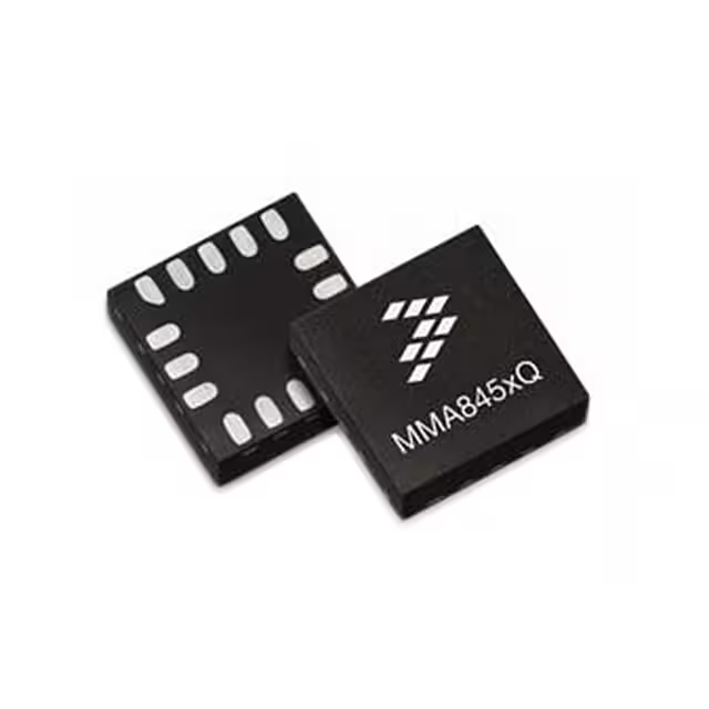
- Part No.:
- MMA8452QR1
- Manufacturer:
- NXP Semiconductors
- Category:
- Accelerometers
- Package:
- 16-VFQFN
- Datasheet:
-
 MMA8452QR1.pdf
- Description:
- ACCELEROMETER 2-8G I2C 16QFN
- Quantity:
- Payment:

- Shipping:

Inventory:2,277
Please send an inquiry. Send us your inquiry, and we will respond immediately.
Product details
Overview
MMA8452QR1 from NXP Semiconductors is a smart, low-power, 3-axis capacitive MEMS accelerometer with 12-bit/8-bit digital output, I²C interface, ±2 g/±4 g/±8 g user-selectable full-scale range, and embedded motion detection logic including freefall, pulse, transient, and orientation (portrait/landscape) functions. It operates from 1.95 V to 3.6 V, consumes as low as 6 μA in low-power mode, and resides in a 3 mm × 3 mm × 1 mm QFN-16 package - deployed in notebook tumble detection, e-reader orientation sensing, and portable device auto-wake systems.
For engineers reviewing the MMA8452QR1 datasheet, MMA8452QR1 pinout, MMA8452QR1 application, or MMA8452QR1 equivalent, this page delivers verified technical context, real-time high-pass filtered data availability, interrupt-driven inertial wakeup capability, configurable ODR from 1.56 Hz to 800 Hz, and confirmed pin-level I²C timing compliance per NXP Rev. 10 (04/2016).
Technical Context
The MMA8452QR1 integrates a 12-bit sigma-delta ADC with programmable oversampling and a dedicated low-noise mode (LNOISE bit), limiting dynamic range to ±4 g when enabled. Its embedded DSP block executes real-time orientation detection using fixed 30°/60° hysteresis thresholds and supports directional pulse detection with debounce counters for reliable tap recognition.
Two open-drain interrupt pins (INT1, INT2) are independently configurable for six sources: freefall, motion, pulse, transient, orientation change, and data-ready events. The device transitions between active, standby, and auto-sleep modes via register-controlled SYSMOD states, enabling host processor offload during inactivity while maintaining sub-1 ms wake latency.
Key Specifications
| Parameter | Value and Actual Design Meaning |
|---|---|
| Supply Voltage | 1.95 V to 3.6 V - powers analog core and enables operation across single-cell Li-ion and dual-cell alkaline systems. |
| I/O Voltage Range | 1.62 V to 3.6 V - supports mixed-voltage host interfaces without level shifters. |
| Full-Scale Range | ±2 g / ±4 g / ±8 g - selectable via FS[1:0] bits; sensitivity scales inversely (1024/512/256 counts/g) for optimal resolution per application. |
| Output Data Rate | 1.56 Hz to 800 Hz - determines trade-off between current draw (6–165 μA) and temporal resolution for motion event capture. |
| RMS Noise Density | 99 μg/√Hz (low-noise mode) - enables detection of subtle vibrations and low-amplitude gestures in battery-constrained devices. |
| Digital Output | 12-bit or 8-bit I²C - 12-bit provides 1 mg LSB at ±2 g; 8-bit reduces bus traffic by reading only MSB registers (F_READ=1). |
| Interrupt Sources | Six configurable: freefall, motion, pulse, transient, orientation, data-ready - allows prioritized event handling without host polling. |
Pinout & Package
Package: 16-pin QFN, 3 mm × 3 mm × 1 mm, exposed thermal pad (GND-connected), RoHS-compliant.
| Pin/Terminal | Circuit Role | Design Meaning |
|---|---|---|
| VDD | Analog power supply input | 1.95–3.6 V main supply; decoupling requires 0.1 μF + 4.7 μF near Pins 1 & 14. |
| VDDIO | Digital I/O power supply | 1.62–3.6 V interface rail; sets logic thresholds for SCL/SDA/SA0; tolerant of voltage sequencing. |
| BYP | Bypass capacitor connection | Accepts 75–470 nF ceramic cap; stabilizes internal oscillator and ADC reference. |
| SCL / SDA | I²C clock/data lines | Open-drain, require external pull-ups; compliant with I²C fast-mode (≤400 kHz); VIH/VIL referenced to VDDIO. |
| SA0 | I²C address LSB | Selects 7-bit slave address: 0x1C (SA0 = 0) or 0x1D (SA0 = 1); enables dual-device addressing on same bus. |
| INT1 / INT2 | Programmable interrupt outputs | Open-drain, 0.1×VDDIO low-level; drive external MCU interrupts; support simultaneous event notification. |
| GND (Pins 5, 10, 12) | Ground reference | Three dedicated GND pins reduce ground impedance and improve noise immunity in high-resolution mode. |
| NC / DNC | No-connect / do-not-connect | Pins 3 (DNC), 8/13/15/16 (NC) must remain unconnected; Pin 16 may optionally connect to GND or VDD per layout needs. |
Key Features
| Feature | Design Value |
|---|---|
| Embedded orientation detection | Portrait/landscape classification with fixed 30°/60° hysteresis thresholds - eliminates need for host-side tilt calculation and reduces firmware overhead. |
| Auto-wake/sleep mode | Configurable transition between low-power (6 μA @ 1.56 Hz) and high-rate (165 μA @ 800 Hz) sampling - extends battery life in always-on portable devices. |
| Real-time high-pass filtered data | Available simultaneously with raw acceleration - enables transient detection (e.g., drop impact) without host-side digital filtering latency. |
| Self-test functionality | Electrostatic actuation verifies transducer integrity at power-up or runtime - confirms sensor health without mechanical stimulus or calibration jig. |
| Three-channel motion detection | Dedicated hardware blocks for freefall/motion, pulse, and transient events - allows concurrent, low-latency event monitoring with independent thresholds and timing. |
Applications
| Smartphone Auto-Rotate | Notebook Freefall Protection |
|---|---|
Use Scenario: Real-time screen rotation triggered by device tilt during handheld use. IC Role / Device Role / Timing Role: MMA8452QR1 continuously monitors X/Y/Z axes and asserts INT1 on portrait-to-landscape transition with 30° hysteresis. Use Value: Enables seamless UI responsiveness with <100 ms orientation update latency and <6 μA background current draw. |
Use Scenario: Immediate HDD head parking upon detecting uncontrolled vertical acceleration during laptop drop. IC Role / Device Role / Timing Role: MMA8452QR1 runs freefall detection (threshold ≤500 mg, duration ≥20 ms) and triggers INT2 within 350 µs of valid voltage ramp. Use Value: Prevents disk damage by initiating mechanical shutdown before impact - validated per MIL-STD-810G shock profiles. |
| Wearable Step Counter | Industrial Shock Monitor |
Use Scenario: Accurate pedometer function in fitness bands using directional pulse detection for step validation. IC Role / Device Role / Timing Role: MMA8452QR1 configures pulse detection channel with directional filtering and 100 ms debounce to reject false triggers from arm swing noise. Use Value: Delivers >95% step-count accuracy at 50 Hz ODR while consuming only 24 μA - extends battery life to 14+ days. |
Use Scenario: Logging vibration amplitude and frequency during shipping of precision equipment to validate warranty claims. IC Role / Device Role / Timing Role: MMA8452QR1 captures transient acceleration spikes (>2 g, >10 ms) via high-pass filtered output and stores timestamps in host memory. Use Value: Provides traceable, timestamped shock event records with 99 μg/√Hz noise floor - meets ISO 13373-3 condition monitoring standards. |
Equivalent & Alternatives
The following parts are listed as comparable options for similar 3-axis digital accelerometer applications.
| Alternative Part | Technical Difference | Application Difference | Selection Advice |
|---|---|---|---|
| MMA8451QT | 14-bit resolution, 4096 counts/g sensitivity, 32-level FIFO, programmable orientation thresholds | Better suited for high-precision tilt measurement and buffered burst-read applications (e.g., drone IMU pre-processing) | Select MMA8451QT when higher resolution and FIFO buffering are required; MMA8452QR1 remains optimal for cost-sensitive, interrupt-driven gesture control. |
| KX122-1037 | 2.5 V to 3.6 V supply, 14-bit output, integrated wake-up engine, lower typical current (4.5 μA @ 1.56 Hz) | Superior ultra-low-power performance and smaller 2 mm × 2 mm LGA package - ideal for space-constrained wearables | Choose KX122-1037 for sub-5 μA standby operation and footprint reduction; MMA8452QR1 offers broader interrupt flexibility and NXP's mature ecosystem support. |
Compared with MMA8451QT and KX122-1037, the MMA8452QR1 delivers balanced performance across resolution (12-bit), interrupt richness (6 sources), and power (6–165 μA), making it the preferred choice for mid-tier consumer electronics requiring robust motion event handling without FIFO or ultra-low-quiescent demands.
Availability
MMA8452QR1 is available at Aetrix Electronics and suitable for notebook tumble detection, e-reader orientation sensing, and smartphone auto-wake applications requiring stable component supply across industrial temperature ranges (–40°C to +85°C).
Supply support for MMA8452QR1 includes scheduled delivery planning, volume procurement assistance, BOM continuity management, traceable sourcing, and lifecycle availability coordination for OEM customers, industrial embedded developers, connected-device designers, and electronics production programs.
Manufacturer
NXP Semiconductors is a global semiconductor leader specializing in secure connectivity solutions for automotive, industrial, and IoT markets, with over 50 years of analog and sensor IP heritage.
The MMA8452QR1 belongs to NXP's "MMA845xQ" family of intelligent accelerometers designed specifically for power-efficient, event-driven motion sensing in portable and battery-operated systems - emphasizing embedded intelligence over raw data streaming.
FAQ
What is the operating temperature range for the MMA8452QR1?
The MMA8452QR1 is rated for continuous operation from –40°C to +85°C, matching the industrial temperature grade specified in its ordering information. This range is validated per NXP's absolute maximum ratings and electrical characteristics tables, ensuring reliable performance in harsh environments such as automotive infotainment mounts or outdoor portable devices. The MMA8452QR1 maintains specified zero-g offset accuracy (±20 mg post-board mount) and sensitivity stability across this full span.
Does the MMA8452QR1 support both 12-bit and 8-bit output modes?
Yes, the MMA8452QR1 supports both 12-bit and 8-bit digital output formats. In 12-bit mode, acceleration data is stored across MSB/LSB registers (e.g., OUT_X_MSB/OUT_X_LSB); in 8-bit mode, only the MSB registers (OUT_X, OUT_Y, OUT_Z) are read after setting the F_READ bit in CTRL_REG1. This reduces I²C transaction count and host processing load - particularly useful in resource-constrained microcontrollers where full resolution is unnecessary.
How does the MMA8452QR1 achieve ultra-low power consumption?
The MMA8452QR1 achieves ultra-low power consumption through multiple hardware-enforced strategies: configurable output data rates (ODR) down to 1.56 Hz, dedicated low-power mode (6 μA), auto-sleep/wake transitions triggered by inertial events, and selective block disabling (e.g., analog subsystem off in standby). Its internal oscillator and ADC architecture minimize switching losses, and the absence of external clocks or complex signal conditioning further reduces system-level power overhead - all confirmed in Table 3 of the NXP Rev. 10 datasheet.
Can the MMA8452QR1 detect directional taps or double-taps?
Yes, the MMA8452QR1 includes dedicated hardware for single-, double-, and directional pulse detection - one of three embedded motion channels. Directional pulse detection uses X/Y/Z axis correlation and configurable thresholds to distinguish left/right/up/down taps, while double-tap logic enforces inter-pulse timing windows (programmable via debounce counters). These functions operate autonomously and assert INT1 or INT2 without host intervention, as detailed in Section 5.7 and Register Map 0x2E–0x31 of the datasheet.
What is the purpose of the BYP pin on the MMA8452QR1?
The BYP pin on the MMA8452QR1 connects to a 0.1 μF ceramic bypass capacitor that stabilizes the internal oscillator and ADC reference voltage. Per NXP's layout guidance, this capacitor must be placed as close as possible to Pin 2 (BYP) and tied to a clean ground plane. Using the recommended 75–470 nF range ensures proper startup timing (≤500 µs boot time), low-noise operation, and immunity to supply ripple - deviations risk timing errors or increased RMS noise beyond the specified 99 μg/√Hz.
MMA8452QR1 Specifications
- Product attributes
- Attribute value
- Manufacturer:
- NXP Semiconductors
- Series:
- -
- Package/Case:
- 16-VFQFN
- Packaging:
- Tape & Reel (TR)
- Product Status:
- Obsolete
- Type:
- Digital
- Axis:
- X, Y, Z
- Acceleration Range:
- ±2g, 4g, 8g
- Sensitivity (LSB/g):
- 1024 (±2g) ~ 256 (±8g)
- Sensitivity (mV/g):
- -
- Bandwidth:
- 0.78Hz ~ 400Hz
- Output Type:
- I2C
- Voltage - Supply:
- 1.95V ~ 3.6V
- Features:
- Adjustable Bandwidth, Selectable Scale, Sleep Mode
- Operating Temperature:
- -40°C ~ 85°C
- Grade:
- -
- Qualification:
- -
- Mounting Type:
- Surface Mount
- Supplier Device Package:
- 16-QFN (3x3)
MMA8452QR1 FAQ
1.How can I place an order for MMA8452QR1 through Aetrix?
Please submit a Request for Quotation (RFQ) for MMA8452QR1 on Aetrix. Our sales agent will provide a competitive quotation and guide you through the order confirmation once you accept the terms.
2.Are the price and stock information for MMA8452QR1 reliable?
The price and inventory of MMA8452QR1 are updated periodically and may fluctuate due to market conditions. Stock and pricing data are typically refreshed every 24 hours. Quotation validity for MMA8452QR1 is usually 5 days.
3.What payment methods are accepted for MMA8452QR1?
We accept Wire Transfer, PayPal, Credit Card, Western Union, MoneyGram, and Escrow for MMA8452QR1 transactions.
Note: Certain payment methods may incur a processing fee.
4.How is shipping managed for MMA8452QR1?
MMA8452QR1 orders can be shipped via leading logistics carriers, including DHL, UPS, FedEx, TNT, or Registered Mail.
Once your MMA8452QR1 order is processed, you will receive an email with the shipment details and tracking number.
Note: Tracking information may take up to 24 hours to appear. Express delivery typically takes 3–5 business days.
5.How can I obtain technical support or documentation for MMA8452QR1?
For technical support, including MMA8452QR1 datasheets, pinout diagrams, or application guidance, please contact our engineering support team. They can provide detailed documentation and assistance for your MMA8452QR1 requirements.
6.How does Aetrix verify that MMA8452QR1 is sourced from the original manufacturer or authorized distributors?
All MMA8452QR1 products on Aetrix are procured from qualified distributors and authorized channels. Our dedicated quality assurance team conducts strict verification, including traceability checks and, if necessary, third-party testing. This ensures that MMA8452QR1 meets industry standards.
7.What is the process for return or replacement of MMA8452QR1?
All MMA8452QR1 units undergo pre-shipment inspection (PSI). If there is an issue with MMA8452QR1, returns or replacements are accepted under the following conditions:
1.Quantity discrepancies, incorrect items, or visible external defects (such as breakage or corrosion), acknowledged by Aetrix.
2.The issue is reported within 90 days of delivery.
3.The MMA8452QR1 part is unused and in its original packaging.
Return procedure for MMA8452QR1:
1.Submit a request within 90 days.
2.Obtain a Return Material Authorization (RMA) from Aetrix.
MMA8452QR1 Tags

-
MXC4005XC
Memsic Inc.

-
MC3419
Memsic Inc.

-
MC3479
Memsic Inc.

-
MXC6655XA
Memsic Inc.

-
MC3630
Memsic Inc.
.jpg)
-
LIS2HH12TR
STMicroelectronics

-
KX122-1037
Kionix Inc.
-
LIS2DE12TR
STMicroelectronics
-
LIS2DH12TR
STMicroelectronics

-
MC3635
Memsic Inc.
-
LIS2DS12TR
STMicroelectronics

-
LIS3DHTR
STMicroelectronics
Tech Hub

A practical engineering guide to 3.3V and 5V logic compatibility, input thresholds, resistor dividers, translator ICs, MOSFET level shifting, I2C pull-ups, timing limits and power-sequencing risks.

The 74HC595 uses push-pull logic outputs, while the TPIC6B595 uses 50 V open-drain DMOS sinks for higher-power loads. This guide compares timing, current limits, 3.3 V interfacing, load wiring, thermal…

The 74HC595 converts serial data into eight stable parallel outputs. This guide covers pin functions, shift and storage timing, OE and MR behavior, drive-current limits, cascading, voltage compatibilit…

A technical comparison of level-sensitive latches and edge-triggered flip-flops, covering timing windows, setup and hold limits, master–slave operation, time borrowing, race-through, HDL inference and…

A D latch stores one bit while Enable controls when data can pass. This reference covers gate-level operation, truth tables, transparency, setup and hold timing, LE versus OE, common ICs and practical …

An SR latch stores one bit through cross-coupled feedback. This engineering reference covers NOR and NAND implementations, truth tables, forbidden-state recovery, gated operation, switch debouncing, fa…

Latch circuits retain one bit through feedback. This technical reference covers SR and D latches, truth tables, transparency, timing limits, latch-versus-flip-flop behavior, applications and common log…

An engineering guide to LED driver operation, constant-current and constant-voltage outputs, linear and switching topologies, dimming, IC selection, calculations, replacement compatibility, and fault c…

Operational amplifier guide covering op amp basics, feedback, ideal vs real op amps, common configurations, buffer circuits, offset, bias current, gain-bandwidth, slew rate, rail-to-rail limits and sel…

Jumper cables guide covering safe connection order, red and black clamp placement, final ground connection, cable gauge, length, clamp quality, copper vs CCA cables, jump starter comparison and battery…


