
 My Inquiry
 My Account


NXP Semiconductors MMA8653FCR1
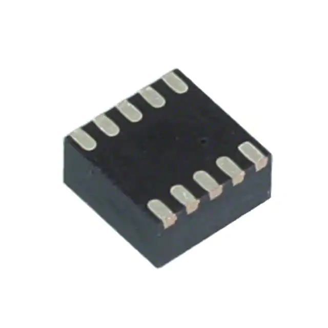
- Part No.:
- MMA8653FCR1
- Manufacturer:
- NXP Semiconductors
- Category:
- Accelerometers
- Package:
- 10-VFDFN
- Datasheet:
-
 MMA8653FCR1.pdf
- Description:
- ACCELEROMETER 2-8G I2C 10DFN
- Quantity:
- Payment:

- Shipping:

Inventory:4,209
Please send an inquiry. Send us your inquiry, and we will respond immediately.
Product details
Overview
MMA8653FCR1 from NXP (formerly Freescale) is a 3-axis, 10-bit digital capacitive MEMS accelerometer in a 10-pin DFN (2 mm × 2 mm × 1 mm) package, operating from 1.95 V to 3.6 V supply and supporting ±2 g / ±4 g / ±8 g full-scale ranges. It delivers output data rates from 1.56 Hz to 800 Hz via I²C interface and integrates embedded orientation detection (Portrait/Landscape with 15° hysteresis), freefall interrupt, and Auto-WAKE/SLEEP mode - enabling inertial event monitoring in ultra-low-power mobile and portable systems.
For engineers reviewing the MMA8653FCR1 datasheet, MMA8653FCR1 pinout, MMA8653FCR1 application, or MMA8653FCR1 equivalent, this page provides verified technical context, confirmed pin functions, real-world use cases for tilt compensation and drop detection, and validated alternative parts with documented functional differences.
Technical Context
The MMA8653FCR1 implements a low-power analog front-end with C-to-V conversion, anti-aliasing filtering, and a 10-bit successive-approximation ADC. Its embedded logic supports configurable motion-triggered interrupts (Freefall, Orientation, Data Ready, Auto-WAKE) routed to two dedicated open-drain outputs (INT1/INT2).
It operates in ACTIVE (WAKE/SLEEP), STANDBY, and OFF modes, with current consumption as low as 6.5 µA in Low Power mode at 1.563 Hz ODR. Orientation detection uses fixed-angle thresholds (±45° midpoint, ±15° hysteresis) and Z-lockout logic to suppress false transitions near flat orientation.
Key Specifications
| Parameter | Value and Actual Design Meaning |
|---|---|
| Supply Voltage | 1.95 V to 3.6 V - powers analog core; enables direct integration with 2.5 V or 3.3 V system rails without LDO overhead. |
| Digital Interface Voltage | 1.62 V to 3.6 V - independent VDDIO allows interfacing with 1.8 V or 3.3 V microcontrollers without level shifters. |
| Full-Scale Range | ±2 g / ±4 g / ±8 g - user-selectable via register; ±2 g mode yields 256 LSB/g sensitivity for high-resolution tilt sensing. |
| Output Data Rate | 1.56 Hz to 800 Hz - programmable ODR supports both ultra-low-power logging (e.g., 1.56 Hz standby) and responsive motion capture (e.g., 800 Hz gaming). |
| Resolution | 10-bit digital output - provides 1,024 discrete levels; LSB values range from 3.9 mg (±2 g) to 15.6 mg (±8 g) for precise acceleration quantization. |
| I²C Interface | Standard/Fast Mode (up to 400 kHz) - 7-bit slave address 0x1D; open-drain SDA/SCL require external pull-ups to VDDIO. |
| Interrupt Outputs | Two programmable open-drain pins (INT1, INT2) - support simultaneous routing of up to four interrupt sources (Data Ready, Freefall, Orientation, Auto-WAKE). |
Pinout & Package
Package: 10-pin DFN (2 mm × 2 mm × 1 mm), case 98ASA00301D, exposed pad not electrically connected. RoHS-compliant, moisture-sensitive level 3.
| Pin/Terminal | Circuit Role | Design Meaning |
|---|---|---|
| 1 - VDD | Analog power supply | Primary supply for internal regulators, transducers, and analog circuitry; requires local 0.1 µF decoupling. |
| 2 - SCL | I²C clock input | Open-drain input; must be pulled up to VDDIO; not tolerant above VDDIO + 0.3 V. |
| 3 - INT1 | Programmable interrupt output | Open-drain output; configurable for Freefall, Orientation, Data Ready, or Auto-WAKE events. |
| 4 - BYP | Internal regulator bypass | Connects to 100 nF capacitor (75–470 nF valid); stabilizes internal LDO for noise-sensitive analog operation. |
| 5 - INT2 | Programmable interrupt output | Second open-drain interrupt output; independently configurable from INT1 for dual-event notification. |
| 6 - GND | Analog ground | Primary ground reference for transducer and analog signal chain; tied to exposed pad internally. |
| 7 - GND | Ground | Secondary ground connection; improves thermal dissipation and reduces ground impedance. |
| 8 - VDDIO | Digital I/O supply | Supplies I²C interface and interrupt drivers; voltage sets logic thresholds for SCL/SDA/INT pins. |
| 9 - GND | Ground | Third ground terminal; enhances PCB grounding integrity and EMI resilience. |
| 10 - SDA | I²C data bidirectional line | Open-drain bidirectional data line; shares pull-up with SCL; requires same VDDIO-compatible voltage domain. |
Key Features
| Feature | Design Value |
|---|---|
| Embedded Portrait/Landscape Detection | Fixed 45° trip point with ±15° hysteresis and Z-lockout logic - eliminates screen flicker during slow rotation near horizontal orientation. |
| Auto-WAKE/SLEEP Mode | Configurable transition between low-ODR (1.56 Hz, 6.5 µA) and high-ODR (800 Hz, 184 µA) based on motion activity - extends battery life in always-on portable devices. |
| Freefall Interrupt Generation | Detects sustained sub-threshold acceleration (< ±500 mg) across all axes for ≥ user-defined time - enables HDD protection and drop-responsive UI behavior. |
| Self-Test Functionality | Electrostatic actuation verifies transducer and signal chain integrity without mechanical stimulus - supports production test and field diagnostics. |
| Factory-Calibrated Offset & Sensitivity | Trim values stored in NVM and auto-applied at boot - eliminates need for end-system calibration in most applications. |
Applications
| Tilt Compensation in e-Compass Systems | Static Orientation Detection for Mobile Devices |
|---|---|
Use Scenario: Compensating magnetometer heading errors caused by device tilt in handheld navigation units. IC Role / Device Role / Timing Role: Provides real-time 3-axis gravity vector to compute pitch/roll angles used in sensor fusion algorithms. Use Value: Enables accurate compass heading within ±2° over ±45° tilt range using fixed hysteresis and Z-lockout to reject false transitions. |
Use Scenario: Detecting device position (Portrait/Landscape/Up/Down/Left/Right/Back/Front) in smartphones and tablets for UI auto-rotation. IC Role / Device Role / Timing Role: Delivers orientation status via interrupt-driven polling, reducing host CPU wake cycles. Use Value: Achieves smooth, jitter-free screen rotation with 15° hysteresis and guaranteed detection above 29° from flat orientation. |
| Notebook/Tablet Freefall & Tumble Detection | Portable Product Power Management |
Use Scenario: Initiating hard disk drive (HDD) head parking or SSD write-protection upon sudden drop or impact in laptops and 2-in-1 devices. IC Role / Device Role / Timing Role: Generates Freefall interrupt within 350–500 µs of valid voltage application, triggering immediate firmware response. Use Value: Supports reliable drop detection down to ±100 mg threshold with configurable duration, meeting MIL-STD-810G shock survivability requirements. |
Use Scenario: Enabling Auto-SLEEP and Auto-WAKE in wearables and remote controls to minimize active time of host MCU. IC Role / Device Role / Timing Role: Monitors inertial activity while consuming only 6.5 µA in Low Power mode, waking host on orientation or motion event. Use Value: Extends battery life by >10× compared to continuous polling, with deterministic wake latency under 2/ODR + 1 ms. |
Equivalent & Alternatives
The following parts are listed as comparable options for similar 3-axis digital accelerometer applications.
| Alternative Part | Technical Difference | Application Difference | Selection Advice |
|---|---|---|---|
| KX122-1037 (Kionix) | 14-bit resolution, ±2 g / ±4 g / ±8 g ranges, 16 µA @ 1.56 Hz, integrated FIFO, no orientation detection logic. | Lacks built-in Portrait/Landscape algorithm; requires host-side processing for orientation - increases MCU load and latency. | Choose when higher resolution and FIFO buffering outweigh need for autonomous orientation interrupts. |
| BMA253 (Bosch Sensortec) | 14-bit output, ±2 g / ±4 g / ±8 g / ±16 g ranges, 140 µA @ 100 Hz, integrated any-motion and no-motion detection, 32-level FIFO. | Supports programmable orientation detection (not fixed-angle), but consumes ~2× more current than MMA8653FCR1 in equivalent low-power mode. | Prefer when flexible multi-threshold motion detection and wider dynamic range are required, and power budget allows. |
Compared with KX122-1037 and BMA253, the MMA8653FCR1 offers uniquely low quiescent current (6.5 µA) with autonomous fixed-angle orientation and freefall detection - making it optimal for battery-constrained devices where deterministic, low-overhead inertial event handling is critical.
Availability
MMA8653FCR1 is available at Aetrix Electronics and suitable for notebook tumble detection, tablet orientation management, and wearable activity monitoring requiring stable component supply and long-term industrial availability.
Supply support for MMA8653FCR1 includes scheduled delivery planning, volume procurement assistance, BOM continuity management, traceable sourcing, and lifecycle availability coordination for OEM customers, industrial embedded developers, connected-device designers, and electronics production programs.
Manufacturer
NXP Semiconductors is a global semiconductor leader focused on secure connectivity solutions for automotive, industrial, and IoT applications, with deep expertise in sensor signal conditioning and embedded intelligence.
The MMA8653FCR1 belongs to NXP's Xtrinsic™ family of intelligent sensors - designed specifically for energy-efficient, event-driven motion awareness in portable and battery-powered electronics.
FAQ
What is the minimum supply voltage required for stable operation of the MMA8653FCR1?
The MMA8653FCR1 requires a minimum supply voltage of 1.95 V on VDD for guaranteed operation across its full temperature range (–40°C to +85°C). Below this threshold, analog performance degrades and register access may become unreliable. The MMA8653FCR1 also supports a separate digital interface supply (VDDIO) down to 1.62 V, allowing interoperability with low-voltage microcontrollers without level-shifting circuitry.
How does the MMA8653FCR1 achieve ultra-low power consumption in motion-sensing applications?
The MMA8653FCR1 achieves ultra-low power consumption through its Auto-WAKE/SLEEP architecture: it remains in a 6.5 µA Low Power mode at 1.56 Hz ODR until triggered by an enabled interrupt source (e.g., Freefall or Orientation change), then automatically transitions to higher ODR for event capture. This eliminates continuous polling and reduces average current by orders of magnitude - a key enabler for multi-year battery life in wearables and remote controls using the MMA8653FCR1.
Can the MMA8653FCR1 detect orientation changes while lying flat on a surface?
No - the MMA8653FCR1 implements Z-lockout logic that disables orientation detection when the Z-axis output falls within ±29° of horizontal (i.e., |Z| < 0.48 g), preventing false portrait/landscape transitions during slow tabletop rotation. This behavior is fixed in silicon and cannot be disabled; it ensures robust operation in real-world usage where devices often rest flat before being lifted or tilted.
What is the function of the BYP pin on the MMA8653FCR1, and what capacitor value is recommended?
Pin 4 (BYP) connects to the output of the internal LDO regulator that powers the analog sensor core. A 100 nF ceramic capacitor (75–470 nF acceptable) must be placed between BYP and GND to stabilize regulation and suppress noise coupling into the transducer signal path. Omitting or undersizing this capacitor causes increased output noise and degraded zero-g offset stability - directly impacting tilt accuracy in the MMA8653FCR1.
Does the MMA8653FCR1 support self-test, and how is it activated?
Yes, the MMA8653FCR1 includes a factory-trimmed electrostatic self-test function. It is activated by setting the SELF bit (bit 0) in the CTRL_REG2 register (0x2B). When enabled, the device applies an internal force simulating acceleration, producing predictable DC-level shifts in the X/Y/Z output registers (e.g., +22.5 LSB on X in ±2 g mode). This allows full signal-chain verification - transducer, C-to-V, ADC, and register readback - without mechanical stimulus, confirming MMA8653FCR1 functionality during production test or field diagnostics.
MMA8653FCR1 Specifications
- Product attributes
- Attribute value
- Manufacturer:
- NXP Semiconductors
- Series:
- -
- Package/Case:
- 10-VFDFN
- Packaging:
- Tape & Reel (TR)
- Product Status:
- Obsolete
- Type:
- Digital
- Axis:
- X, Y, Z
- Acceleration Range:
- ±2g, 4g, 8g
- Sensitivity (LSB/g):
- 256 (±2g) ~ 64 (±8g)
- Sensitivity (mV/g):
- -
- Bandwidth:
- 0.782Hz ~ 400Hz
- Output Type:
- I2C
- Voltage - Supply:
- 1.95V ~ 3.6V
- Features:
- -
- Operating Temperature:
- -40°C ~ 85°C
- Grade:
- -
- Qualification:
- -
- Mounting Type:
- Surface Mount
- Supplier Device Package:
- 10-DFN (2x2)
MMA8653FCR1 FAQ
1.How can I place an order for MMA8653FCR1 through Aetrix?
Please submit a Request for Quotation (RFQ) for MMA8653FCR1 on Aetrix. Our sales agent will provide a competitive quotation and guide you through the order confirmation once you accept the terms.
2.Are the price and stock information for MMA8653FCR1 reliable?
The price and inventory of MMA8653FCR1 are updated periodically and may fluctuate due to market conditions. Stock and pricing data are typically refreshed every 24 hours. Quotation validity for MMA8653FCR1 is usually 5 days.
3.What payment methods are accepted for MMA8653FCR1?
We accept Wire Transfer, PayPal, Credit Card, Western Union, MoneyGram, and Escrow for MMA8653FCR1 transactions.
Note: Certain payment methods may incur a processing fee.
4.How is shipping managed for MMA8653FCR1?
MMA8653FCR1 orders can be shipped via leading logistics carriers, including DHL, UPS, FedEx, TNT, or Registered Mail.
Once your MMA8653FCR1 order is processed, you will receive an email with the shipment details and tracking number.
Note: Tracking information may take up to 24 hours to appear. Express delivery typically takes 3–5 business days.
5.How can I obtain technical support or documentation for MMA8653FCR1?
For technical support, including MMA8653FCR1 datasheets, pinout diagrams, or application guidance, please contact our engineering support team. They can provide detailed documentation and assistance for your MMA8653FCR1 requirements.
6.How does Aetrix verify that MMA8653FCR1 is sourced from the original manufacturer or authorized distributors?
All MMA8653FCR1 products on Aetrix are procured from qualified distributors and authorized channels. Our dedicated quality assurance team conducts strict verification, including traceability checks and, if necessary, third-party testing. This ensures that MMA8653FCR1 meets industry standards.
7.What is the process for return or replacement of MMA8653FCR1?
All MMA8653FCR1 units undergo pre-shipment inspection (PSI). If there is an issue with MMA8653FCR1, returns or replacements are accepted under the following conditions:
1.Quantity discrepancies, incorrect items, or visible external defects (such as breakage or corrosion), acknowledged by Aetrix.
2.The issue is reported within 90 days of delivery.
3.The MMA8653FCR1 part is unused and in its original packaging.
Return procedure for MMA8653FCR1:
1.Submit a request within 90 days.
2.Obtain a Return Material Authorization (RMA) from Aetrix.
MMA8653FCR1 Tags

-
MXC4005XC
Memsic Inc.

-
MC3419
Memsic Inc.

-
MC3479
Memsic Inc.

-
MXC6655XA
Memsic Inc.

-
MC3630
Memsic Inc.
.jpg)
-
LIS2HH12TR
STMicroelectronics

-
KX122-1037
Kionix Inc.
-
LIS2DE12TR
STMicroelectronics
-
LIS2DH12TR
STMicroelectronics

-
MC3635
Memsic Inc.
-
LIS2DS12TR
STMicroelectronics

-
LIS3DHTR
STMicroelectronics
Tech Hub

A practical engineering guide to 3.3V and 5V logic compatibility, input thresholds, resistor dividers, translator ICs, MOSFET level shifting, I2C pull-ups, timing limits and power-sequencing risks.

The 74HC595 uses push-pull logic outputs, while the TPIC6B595 uses 50 V open-drain DMOS sinks for higher-power loads. This guide compares timing, current limits, 3.3 V interfacing, load wiring, thermal…

The 74HC595 converts serial data into eight stable parallel outputs. This guide covers pin functions, shift and storage timing, OE and MR behavior, drive-current limits, cascading, voltage compatibilit…

A technical comparison of level-sensitive latches and edge-triggered flip-flops, covering timing windows, setup and hold limits, master–slave operation, time borrowing, race-through, HDL inference and…

A D latch stores one bit while Enable controls when data can pass. This reference covers gate-level operation, truth tables, transparency, setup and hold timing, LE versus OE, common ICs and practical …

An SR latch stores one bit through cross-coupled feedback. This engineering reference covers NOR and NAND implementations, truth tables, forbidden-state recovery, gated operation, switch debouncing, fa…

Latch circuits retain one bit through feedback. This technical reference covers SR and D latches, truth tables, transparency, timing limits, latch-versus-flip-flop behavior, applications and common log…

An engineering guide to LED driver operation, constant-current and constant-voltage outputs, linear and switching topologies, dimming, IC selection, calculations, replacement compatibility, and fault c…

Operational amplifier guide covering op amp basics, feedback, ideal vs real op amps, common configurations, buffer circuits, offset, bias current, gain-bandwidth, slew rate, rail-to-rail limits and sel…

Jumper cables guide covering safe connection order, red and black clamp placement, final ground connection, cable gauge, length, clamp quality, copper vs CCA cables, jump starter comparison and battery…


