
 My Inquiry
 My Account


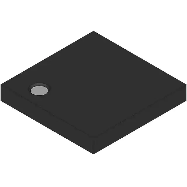
NXP Semiconductors MMA9553LR1
- Part No.:
- MMA9553LR1
- Manufacturer:
- NXP Semiconductors
- Category:
- Accelerometers
- Package:
- 16-VFLGA
- Datasheet:
-
 MMA9553LR1.pdf
- Description:
- ACCELEROMETER 2-8G I2C/SPI 16LGA
- Quantity:
- Payment:

- Shipping:

Inventory:2,853
Please send an inquiry. Send us your inquiry, and we will respond immediately.
Product details
Overview
MMA9553LR1 from NXP Semiconductors (formerly Freescale) is an intelligent, low-power 3-axis motion-sensing platform integrating a MEMS accelerometer, 32-bit ColdFire V1 MCU, 16-KB flash, 2-KB RAM, and programmable firmware preloaded for pedometer functionality. It operates at 1.8 V, supports ±2/±4/±8 g ranges, delivers 10–16-bit ADC resolution, and communicates via slave I²C (7-bit address 0x4C) or SPI to host processors in portable consumer devices.
For engineers reviewing the MMA9553LR1 datasheet, MMA9553LR1 pinout, MMA9553LR1 application, or MMA9553LR1 equivalent, this page provides verified technical context, confirmed pin functions, real-world pedometer use cases, validated alternatives, and supply-chain support details specific to the factory-programmed pedometer variant of the MMA955xL family.
Technical Context
The MMA9553LR1 implements a dedicated pedometer firmware stack with step counting, distance estimation, adaptive distance calculation, and activity monitoring - all executed autonomously on its integrated 32-bit CPU without host processor intervention. Its analog front end includes capacitance-to-voltage conversion, temperature sensing, and differential ADC inputs (AN0/AN1) synchronized to accelerometer ODR.
It features dual I²C interfaces: a slave port (SCL0/SDA0, up to 2 Mbps) for host communication and a master port (SCL1/SDA1, up to 400 kbps) for managing external sensors. Power management includes auto-wake/sleep, deep-sleep modes, and hardware-level interrupt generation (INT, INT_O) triggered by motion events.
Key Specifications
| Parameter | Value and Actual Design Meaning |
|---|---|
| Supply Voltage | 1.8 V nominal - powers both digital (VDD/VSS) and analog (VDDA/VSSA) domains; requires separate low-noise bypassing per domain. |
| Accelerometer Ranges | ±2 g, ±4 g, ±8 g - selectable in firmware; ±2 g optimized for orientation/tilt, ±4 g for walking/jogging, ±8 g for abrupt gaming motions. |
| ADC Resolution | 10/12/14/16 bits - configurable per application; higher bit depth enables precise step-detection thresholding and noise rejection. |
| Output Data Rate (ODR) | 3.8 Hz to 488 Hz - eight discrete rates; pedometer firmware uses sub-10 Hz rates to minimize power while maintaining step detection accuracy. |
| I²C Slave Address | Default 7-bit address 0x4C - customizable via firmware; enables multi-device I²C bus integration without address conflict. |
| Memory Resources | 16 KB flash / 2 KB RAM - 1.0 KB user flash and 420 bytes user RAM reserved for custom extensions beyond factory pedometer firmware. |
| Operating Temperature | –40°C to +85°C - qualified for industrial and consumer portable environments including wearables and handhelds. |
Pinout & Package
16-pin LGA package (3 mm × 3 mm × 1 mm, Case 2094-01), RoHS-compliant, with exposed pad for thermal and electrical grounding. All pins are functional and multiplexed; default reset-state functions defined in SIM registers.
| Pin/Terminal | Circuit Role | Design Meaning |
|---|---|---|
| VDD / VSS | Digital power / ground | 1.8 V digital supply pair; requires local 0.01–0.1 µF ceramic bypass capacitor per VDD–VSS pair. |
| VDDA / VSSA | Analog power / ground | 1.8 V analog supply pair; must be filtered separately from digital rails to preserve ADC and accelerometer SNR. |
| SCL0 / SDA0 | Slave I²C clock / data | Host interface port; default 7-bit address 0x4C; supports up to 2 Mbps; pulled high externally via 4.7 kΩ resistors. |
| SCL1 / SDA1 | Master I²C clock / data | External sensor hub interface; operates up to 400 kbps; used to initialize, calibrate, and read pressure/magnetometer data. |
| RESETB | Active-low reset input | Open-drain bidirectional pin; must be pulled high at power-up to boot into application code; asserts system reset when driven low. |
| BKGD-MS | Background-debug / mode select | Pulled high at startup for normal operation; pulled low to enter BDM for firmware download/debug; internal pullup enabled. |
| INT | Interrupt input | Level-7 priority input; wakes CPU from deep-sleep on edge/level; used by host to trigger pedometer data reads or configuration updates. |
| RGPIO4 | Programmable GPIO / interrupt | Configurable as general-purpose input/output or secondary interrupt source; supports rising/falling/level-triggered events. |
Key Features
| Feature | Design Value |
|---|---|
| Factory-programmed pedometer firmware | Delivers production-ready step count, distance, adaptive distance, and activity monitoring - no host CPU computation required. |
| Autonomous sensor hub capability | Offloads pressure/magnetometer initialization, calibration, and compensation from host processor using master I²C interface. |
| Multi-rate, low-power ODR selection | Eight discrete output data rates (3.8–488 Hz) enable precise trade-off between pedometer accuracy and battery life. |
| Dual-domain power isolation | Separate VDDA/VSSA and VDD/VSS rails with independent bypassing reduce analog noise coupling and preserve 16-bit ADC linearity. |
| Hardware-accelerated motion decision engine | On-chip 32-bit CPU with MAC unit executes real-time filtering, thresholding, and event classification - eliminating software overhead on host. |
Applications
| Wearable Fitness Tracker | Smartphone Activity Monitor |
|---|---|
Use Scenario: Continuous step counting and daily activity scoring in wrist-worn trackers with multi-day battery life. IC Role / Device Role / Timing Role: Primary motion decision engine - autonomously detects steps, computes distance, and triggers host wake only upon new activity epoch. Use Value: Reduces host processor duty cycle by >95%, extending battery life while maintaining ±3% step-count accuracy per ISO 20957-3. | Use Scenario: Background activity classification (walking, jogging, idle) alongside GPS and cellular radios in smartphones. IC Role / Device Role / Timing Role: Always-on motion coprocessor - samples at 6.1 Hz, buffers data in embedded FIFO, and signals host only on state transition. Use Value: Enables Android Sensor HAL integration with <10 µA average current draw during activity monitoring. |
| Medical Rehabilitation Logger | Industrial Asset Tracker |
Use Scenario: Quantifying patient ambulation metrics (steps/day, gait symmetry) during post-injury recovery programs. IC Role / Device Role / Timing Role: Calibrated motion logger - applies tilt-compensated step detection and stores timestamped activity bursts in nonvolatile flash. Use Value: Provides clinical-grade step data traceable to NIST-traceable accelerometer calibration, compliant with FDA SaMD guidance. | Use Scenario: Monitoring equipment movement and shock events in logistics containers or field-deployed machinery. IC Role / Device Role / Timing Role: Event-triggered wake controller - sleeps at 0.24 Hz, wakes on >3g shock, logs timestamped acceleration peaks to internal memory. Use Value: Captures tamper/shock events with <50 ms latency and zero host dependency - critical for chain-of-custody reporting. |
Equivalent & Alternatives
The following parts are listed as comparable options for similar pedometer and motion-sensing applications.
| Alternative Part | Technical Difference | Application Difference | Selection Advice |
|---|---|---|---|
| BST-BNO055 | Integrated 9-DOF IMU (accelerometer + gyroscope + magnetometer); 32-bit Cortex-M0+; no factory pedometer firmware. | Requires full custom algorithm development for step counting; supports orientation fusion but adds cost and power overhead. | Select when fused heading, rotation rate, or gesture recognition beyond pedometer is required - not a drop-in replacement. |
| ST LSM6DSOX | 6-DOF IMU with machine-learning core (MLC); 2.5 V to 3.6 V supply; no integrated MCU or pedometer firmware. | Relies on host or MLC for step detection; lacks autonomous decision engine and sensor hub capability of MMA9553LR1. | Choose for ultra-low-power always-on sensing where host offload is acceptable and voltage range flexibility is needed. |
Compared with BST-BNO055 and ST LSM6DSOX, the MMA9553LR1 uniquely delivers production-ready pedometer functionality with autonomous processing, dual I²C sensor hub control, and 1.8 V operation - reducing BOM count, firmware development time, and system-level power by eliminating host-side motion computation.
Availability
MMA9553LR1 is available at Aetrix Electronics and suitable for wearable fitness trackers, smartphone activity monitors, medical rehabilitation loggers, and industrial asset trackers requiring stable component supply, long-term lifecycle support, and factory-validated pedometer performance.
Supply support for MMA9553LR1 includes scheduled delivery planning, volume procurement assistance, BOM continuity management, traceable sourcing, and lifecycle availability coordination for OEM customers, industrial embedded developers, connected-device designers, and electronics production programs.
Manufacturer
NXP Semiconductors is a global semiconductor leader focused on secure connectivity solutions for automotive, industrial, and IoT applications.
The MMA9553LR1 belongs to the MMA955xL intelligent motion-sensing platform product line, designed specifically to offload motion processing from host processors in battery-constrained portable devices through integrated MCU, calibrated sensors, and application-specific firmware.
FAQ
What pedometer functions are preloaded in the factory firmware of the MMA9553LR1?
The MMA9553LR1 ships with factory-programmed firmware enabling step counting, distance estimation, adaptive distance calculation, and activity monitoring - all executed autonomously on its 32-bit ColdFire V1 MCU. No host-side algorithm development is required to deploy basic pedometer functionality. The MMA9553LR1 firmware is distinct from MMA9551LR1 (gesture) and MMA9559LR1 (foundation) variants, and does not include real-time scheduling or event queue features found only in the MMA9559L.
Does the MMA9553LR1 support communication with external sensors like magnetometers or pressure sensors?
Yes, the MMA9553LR1 includes a dedicated master I²C interface (SCL1/SDA1) operating up to 400 kbps, enabling it to initialize, calibrate, and read data from external sensors such as magnetometers or pressure sensors. This capability allows the MMA9553LR1 to act as an intelligent sensor hub, offloading sensor management tasks from the host processor and reducing overall system power consumption.
What is the default I²C slave address of the MMA9553LR1, and can it be changed?
The MMA9553LR1 has a default 7-bit I²C slave address of 0x4C on its SCL0/SDA0 interface. This address can be customized via firmware configuration, allowing multiple MMA9553LR1 devices or other peripherals to coexist on the same I²C bus without address conflict. The change requires reprogramming the device's configuration registers using CodeWarrior Development Studio.
How does the MMA9553LR1 manage power in pedometer applications?
The MMA9553LR1 implements multiple low-power strategies for pedometer use: it operates at 1.8 V, supports deep-sleep modes with wake-on-motion interrupts (INT pin), uses configurable ODR down to 3.8 Hz, and executes all pedometer logic autonomously - keeping the host processor powered down. Its power-management module includes auto-wake/auto-sleep and doze modes, achieving sub-10 µA average current in typical wearable deployments.
Is the MMA9553LR1 pin-compatible with other devices in the MMA955xL family, such as the MMA9551LR1 or MMA9559LR1?
Yes, the MMA9553LR1 shares identical 16-pin LGA packaging (3 mm × 3 mm × 1 mm, Case 2094-01) and pinout with all MMA955xL variants including MMA9551LR1 and MMA9559LR1. Mechanical and electrical pin mapping is fully compatible; differences are limited to factory-loaded firmware and available user memory resources - making hardware design reusable across the family.
MMA9553LR1 Specifications
- Product attributes
- Attribute value
- Manufacturer:
- NXP Semiconductors
- Series:
- -
- Package/Case:
- 16-VFLGA
- Packaging:
- Tape & Reel (TR)
- Product Status:
- Obsolete
- Type:
- Digital
- Axis:
- X, Y, Z
- Acceleration Range:
- ±2g, 4g, 8g
- Sensitivity (LSB/g):
- 16393 (±2g) ~ 4098 (±8g)
- Sensitivity (mV/g):
- -
- Bandwidth:
- 1.9Hz ~ 244Hz
- Output Type:
- I2C, SPI
- Voltage - Supply:
- 1.71V ~ 1.89V
- Features:
- Adjustable Bandwidth, Selectable Scale, Sleep Mode, Temperature Sensor
- Operating Temperature:
- -40°C ~ 85°C
- Grade:
- -
- Qualification:
- -
- Mounting Type:
- Surface Mount
- Supplier Device Package:
- 16-LGA (3x3)
MMA9553LR1 FAQ
1.How can I place an order for MMA9553LR1 through Aetrix?
Please submit a Request for Quotation (RFQ) for MMA9553LR1 on Aetrix. Our sales agent will provide a competitive quotation and guide you through the order confirmation once you accept the terms.
2.Are the price and stock information for MMA9553LR1 reliable?
The price and inventory of MMA9553LR1 are updated periodically and may fluctuate due to market conditions. Stock and pricing data are typically refreshed every 24 hours. Quotation validity for MMA9553LR1 is usually 5 days.
3.What payment methods are accepted for MMA9553LR1?
We accept Wire Transfer, PayPal, Credit Card, Western Union, MoneyGram, and Escrow for MMA9553LR1 transactions.
Note: Certain payment methods may incur a processing fee.
4.How is shipping managed for MMA9553LR1?
MMA9553LR1 orders can be shipped via leading logistics carriers, including DHL, UPS, FedEx, TNT, or Registered Mail.
Once your MMA9553LR1 order is processed, you will receive an email with the shipment details and tracking number.
Note: Tracking information may take up to 24 hours to appear. Express delivery typically takes 3–5 business days.
5.How can I obtain technical support or documentation for MMA9553LR1?
For technical support, including MMA9553LR1 datasheets, pinout diagrams, or application guidance, please contact our engineering support team. They can provide detailed documentation and assistance for your MMA9553LR1 requirements.
6.How does Aetrix verify that MMA9553LR1 is sourced from the original manufacturer or authorized distributors?
All MMA9553LR1 products on Aetrix are procured from qualified distributors and authorized channels. Our dedicated quality assurance team conducts strict verification, including traceability checks and, if necessary, third-party testing. This ensures that MMA9553LR1 meets industry standards.
7.What is the process for return or replacement of MMA9553LR1?
All MMA9553LR1 units undergo pre-shipment inspection (PSI). If there is an issue with MMA9553LR1, returns or replacements are accepted under the following conditions:
1.Quantity discrepancies, incorrect items, or visible external defects (such as breakage or corrosion), acknowledged by Aetrix.
2.The issue is reported within 90 days of delivery.
3.The MMA9553LR1 part is unused and in its original packaging.
Return procedure for MMA9553LR1:
1.Submit a request within 90 days.
2.Obtain a Return Material Authorization (RMA) from Aetrix.
MMA9553LR1 Tags

-
MXC4005XC
Memsic Inc.

-
MC3419
Memsic Inc.

-
MC3479
Memsic Inc.

-
MXC6655XA
Memsic Inc.

-
MC3630
Memsic Inc.
.jpg)
-
LIS2HH12TR
STMicroelectronics

-
KX122-1037
Kionix Inc.
-
LIS2DE12TR
STMicroelectronics
-
LIS2DH12TR
STMicroelectronics

-
MC3635
Memsic Inc.
-
LIS2DS12TR
STMicroelectronics

-
LIS3DHTR
STMicroelectronics
Tech Hub

A practical engineering guide to 3.3V and 5V logic compatibility, input thresholds, resistor dividers, translator ICs, MOSFET level shifting, I2C pull-ups, timing limits and power-sequencing risks.

The 74HC595 uses push-pull logic outputs, while the TPIC6B595 uses 50 V open-drain DMOS sinks for higher-power loads. This guide compares timing, current limits, 3.3 V interfacing, load wiring, thermal…

The 74HC595 converts serial data into eight stable parallel outputs. This guide covers pin functions, shift and storage timing, OE and MR behavior, drive-current limits, cascading, voltage compatibilit…

A technical comparison of level-sensitive latches and edge-triggered flip-flops, covering timing windows, setup and hold limits, master–slave operation, time borrowing, race-through, HDL inference and…

A D latch stores one bit while Enable controls when data can pass. This reference covers gate-level operation, truth tables, transparency, setup and hold timing, LE versus OE, common ICs and practical …

An SR latch stores one bit through cross-coupled feedback. This engineering reference covers NOR and NAND implementations, truth tables, forbidden-state recovery, gated operation, switch debouncing, fa…

Latch circuits retain one bit through feedback. This technical reference covers SR and D latches, truth tables, transparency, timing limits, latch-versus-flip-flop behavior, applications and common log…

An engineering guide to LED driver operation, constant-current and constant-voltage outputs, linear and switching topologies, dimming, IC selection, calculations, replacement compatibility, and fault c…

Operational amplifier guide covering op amp basics, feedback, ideal vs real op amps, common configurations, buffer circuits, offset, bias current, gain-bandwidth, slew rate, rail-to-rail limits and sel…

Jumper cables guide covering safe connection order, red and black clamp placement, final ground connection, cable gauge, length, clamp quality, copper vs CCA cables, jump starter comparison and battery…


