
 My Inquiry
 My Account


NXP Semiconductors NT3H2211W0FT1X
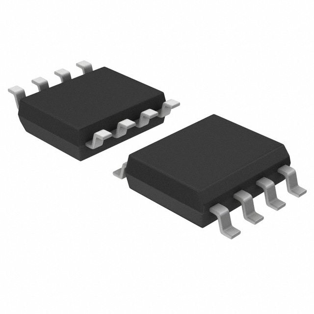
- Part No.:
- NT3H2211W0FT1X
- Manufacturer:
- NXP Semiconductors
- Category:
- RFID, RF Access, Monitoring ICs
- Package:
- 8-SOIC (0.154", 3.90mm Width)
- Datasheet:
-
 NT3H2211W0FT1X.pdf
- Description:
- IC RFID TRANSP 13.56MHZ 8SO
- Quantity:
- Payment:

- Shipping:

Inventory:1,995
Please send an inquiry. Send us your inquiry, and we will respond immediately.
Product details
Overview
NT3H2211W0FT1X from NXP Semiconductors is a second-generation connected NFC tag IC integrating ISO/IEC 14443A-compliant passive NFC interface and I2C slave interface, with 2 kbytes EEPROM, 64-byte SRAM, and energy harvesting output (VOUT) delivering up to 15 mW - enabling tap-and-go configuration and power delivery in home-automation nodes and consumer electronics.
For engineers reviewing the NT3H2211W0FT1X datasheet, NT3H2211W0FT1X pinout, NT3H2211W0FT1X application, or NT3H2211W0FT1X equivalent, key selection considerations include NFC/I2C dual-interface memory arbitration, ECC-based originality signature for anti-cloning, password-protected memory access (32-bit), field-detection (FD) pin for event synchronization, and SO8 package compatibility with legacy PCB layouts.
Technical Context
The NT3H2211W0FT1X implements a dual-interface architecture where NFC and I2C share access to a unified memory map via an internal arbiter, supporting both pass-through and mirror modes. Its digital control unit executes ISO/IEC 14443-3 Type A state machine (IDLE → READY1 → READY2 → ACTIVE → AUTHENTICATED) and interprets standard NFC commands including FAST_READ/FAST_WRITE (64-byte SRAM transfer in 6.1 ms) and GET_VERSION.
Power management integrates energy harvesting from the NFC field into VOUT (capable of powering external microcontrollers), while the FD pin provides open-drain event signaling synchronized to NFC field presence. Memory access is secured via 32-bit password protection per interface, ECC-based originality signature, and configurable lock bits for EEPROM pages and SRAM regions.
Key Specifications
| Parameter | Value and Actual Design Meaning |
|---|---|
| Memory | 2 kbytes EEPROM (20-year data retention, 500k write cycles) + 64-byte SRAM (unlimited endurance, volatile, requires VCC) |
| NFC Interface | ISO/IEC 14443A Type 2 Tag compliant; 106 kbit/s data rate; certified NFC Forum T2T (ID: 58514); 7-byte UID |
| I2C Interface | Slave mode only; 7-bit address (default AAh write / ABh read); supports up to 400 kHz clock; fail-safe operation |
| Energy Harvesting | VOUT pin delivers up to 15 mW from NFC field; enables zero-power system wake-up or MCU biasing without external supply |
| Security | 32-bit password protection per interface; ECC-based originality signature; NFC silence feature; dynamic/static lock bits per memory page |
| Operating Range | −40 °C to +105 °C ambient; input capacitance 50 pF; max operating distance ~100 mm (antenna-dependent) |
| Package | SO8 (SOT96-1); 8-pin plastic small outline; body width 3.9 mm; 1000 pcs/reel |
Pinout & Package
NT3H2211W0FT1X is housed in an SO8 package (SOT96-1), with 8 leads, body width 3.9 mm, and standard gull-wing lead form factor compatible with automated SMT assembly and legacy board footprints.
| Pin/Terminal | Circuit Role | Design Meaning |
|---|---|---|
| 1 LA | NFC antenna terminal A | Connects to one end of external loop antenna coil; forms resonant LC tank with internal capacitance |
| 2 VSS | Ground reference | Common return path for NFC RF circuitry, I2C logic, and energy harvesting regulator |
| 3 SCL | I2C serial clock input | Accepts master-generated clock up to 400 kHz; open-drain compatible; requires external pull-up |
| 4 FD | Field detection output | Open-drain signal asserted low when NFC field is detected; used for wake-up or data-transfer sync |
| 5 SDA | I2C serial data bidirectional | Open-drain bidirectional line; shares pull-up with SCL; supports standard I2C read/write protocols |
| 6 VCC | External power supply input | Required to enable SRAM access and I2C functionality; range 1.8–5.5 V; powers internal logic and regulators |
| 7 VOUT | Energy harvesting output | Regulated output derived from NFC field; supplies up to 15 mW at ~3.3 V to external circuitry |
| 8 LB | NFC antenna terminal B | Connects to opposite end of external loop antenna; completes resonant circuit with LA |
Key Features
| Feature | Design Value |
|---|---|
| Pass-through mode | Enables real-time NFC-to-I2C data relay using 64-byte SRAM buffer - eliminates host MCU polling and reduces latency |
| Memory arbitration | Dedicated hardware arbiter prevents NFC/I2C bus contention; ensures atomic memory access and deterministic behavior |
| ECC originality signature | Provides cryptographic proof of genuine NXP silicon - blocks cloned tags in authentication-critical applications like medical device pairing |
| Configurable access control | Independent 32-bit password enforcement per interface (NFC/I2C), plus per-page lock bits - enables multi-tier security policies |
| Fail-safe I2C | Guarantees bus recovery after clock stretching or SDA/SCL glitches - critical for robust operation in noisy industrial environments |
Applications
| Smart Home Sensors | Consumer Audio Accessories |
|---|---|
Use Scenario: Tap-to-configure temperature/humidity sensor node with Wi-Fi credentials and firmware update URL. IC Role / Device Role / Timing Role: NFC interface receives encrypted provisioning data; I2C transfers it to host MCU; VOUT powers MCU during boot. Use Value: Eliminates manual SSID entry; enables field updates without disassembly; energy harvesting removes battery dependency during setup. |
Use Scenario: Pair Bluetooth speaker with smartphone via NFC tap, then store user EQ profile and firmware version. IC Role / Device Role / Timing Role: Acts as secure, non-volatile configuration hub - NFC initiates pairing, I2C stores persistent settings in EEPROM. Use Value: Reduces pairing time from >30 s to <2 s; ECC signature prevents counterfeit accessories from spoofing device identity. |
| Fitness Equipment | Electronic Shelf Labels (ESL) |
Use Scenario: Gym equipment logs user ID, workout duration, and resistance level via NFC tap before session start. IC Role / Device Role / Timing Role: Stores encrypted user profile and calibration data; FD pin triggers MCU wake-up on field detection. Use Value: Enables personalized training without login screens; 105 °C rating supports operation near motor heat sources. |
Use Scenario: Retail shelf label updated wirelessly via NFC-enabled handheld; price, stock, and promotion data written to tag. IC Role / Device Role / Timing Role: Dual-interface memory serves as bridge - NFC writes new content, I2C refreshes display driver in real time. Use Value: Allows rapid, battery-free updates without wired infrastructure; 2 kbytes EEPROM accommodates multilingual product info. |
Equivalent & Alternatives
The following parts are listed as comparable options for similar connected NFC tag applications.
| Alternative Part | Technical Difference | Application Difference | Selection Advice |
|---|---|---|---|
| NT3H2111W0FT1X | 1 kbyte EEPROM (vs. 2 kbyte), identical SO8 package, same pinout, identical I2C/NFC specs and security features | Suitable for simpler configurations with smaller data payloads (e.g., single-device pairing only) | Select when memory budget is constrained and cost sensitivity outweighs future scalability needs |
| NT3H2211W0FTTJ | TSSOP8 package (3 mm width vs. SO8's 3.9 mm); identical electrical specs, memory, and features | Better suited for space-constrained PCBs where SO8 footprint is too wide; requires layout revision | Choose for new designs prioritizing board area over legacy compatibility; no functional trade-offs |
Compared with NT3H2211W0FT1X, NT3H2111W0FT1X offers identical interface performance and security in a lower-density memory variant, while NT3H2211W0FTTJ delivers identical functionality in a narrower TSSOP8 footprint - enabling design flexibility without compromising NFC/I2C interoperability or energy harvesting capability.
Availability
NT3H2211W0FT1X is available at Aetrix Electronics and suitable for smart home sensors, consumer audio accessories, fitness equipment, and electronic shelf labels requiring stable component supply, long-term lifecycle support, and guaranteed traceable sourcing.
Supply support for NT3H2211W0FT1X includes scheduled delivery planning, volume procurement assistance, BOM continuity management, traceable sourcing, and lifecycle availability coordination for OEM customers, industrial embedded developers, connected-device designers, and electronics production programs.
Manufacturer
NXP Semiconductors is a global semiconductor leader focused on secure connectivity solutions for automotive, industrial, and IoT markets, with deep expertise in NFC, RFID, and secure element technologies.
The NTAG I2C plus product line was designed specifically to enable low-cost, dual-interface NFC integration in resource-constrained embedded systems - combining contactless convenience with wired reliability and energy autonomy.
FAQ
What is the primary function of the FD pin on the NT3H2211W0FT1X?
The FD (Field Detection) pin on the NT3H2211W0FT1X is an open-drain output that asserts low when an NFC field is detected. It enables host MCU wake-up without continuous polling, synchronizes pass-through data transfers between NFC and I2C interfaces, and supports low-power system architectures - a core enabler of zero-power configuration in battery-free devices.
Does the NT3H2211W0FT1X require an external power supply to operate its NFC interface?
No - the NFC interface of the NT3H2211W0FT1X operates entirely passively, powered by energy harvested from the reader's RF field. However, VCC must be supplied (1.8–5.5 V) to enable I2C communication, SRAM access, and VOUT regulation. Without VCC, only basic NFC read/write to EEPROM is functional.
How does memory arbitration work between NFC and I2C on the NT3H2211W0FT1X?
The NT3H2211W0FT1X uses a hardware-based arbiter to manage concurrent NFC and I2C memory access. It prevents bus contention by granting exclusive access per transaction, enforcing priority rules (e.g., NFC commands interrupt ongoing I2C transfers), and maintaining consistent memory state - ensuring deterministic behavior even under mixed-interface load.
Can the NT3H2211W0FT1X be used as a standalone I2C EEPROM without NFC functionality?
Yes - the NT3H2211W0FT1X functions fully as a standard I2C EEPROM (2 kbytes) and I2C SRAM (64 bytes) when VCC is applied, regardless of NFC field presence. Its I2C slave interface supports standard read/write protocols at up to 400 kHz, and all memory protection features (password, locks) remain active and configurable via I2C.
What security mechanisms protect against cloning of the NT3H2211W0FT1X?
The NT3H2211W0FT1X incorporates ECC-based originality signature generation, factory-programmed unique 7-byte UID, one-time programmable capability container bits, and per-page dynamic/static lock bits. These features collectively prevent bit-for-bit cloning and enable cryptographic verification of genuine NXP silicon in authentication-sensitive deployments.
NT3H2211W0FT1X Specifications
- Product attributes
- Attribute value
- Manufacturer:
- NXP Semiconductors
- Series:
- -
- Package/Case:
- 8-SOIC (0.154", 3.90mm Width)
- Packaging:
- Tape & Reel (TR)
- Product Status:
- Active
- Type:
- RFID Transponder
- Frequency:
- 13.56MHz
- Standards:
- ISO 14443
- Interface:
- I2C
- Voltage - Supply:
- 3.3V
- Operating Temperature:
- -40°C ~ 105°C
- Grade:
- -
- Qualification:
- -
- Mounting Type:
- Surface Mount
- Supplier Device Package:
- 8-SO
NT3H2211W0FT1X FAQ
1.How can I place an order for NT3H2211W0FT1X through Aetrix?
Please submit a Request for Quotation (RFQ) for NT3H2211W0FT1X on Aetrix. Our sales agent will provide a competitive quotation and guide you through the order confirmation once you accept the terms.
2.Are the price and stock information for NT3H2211W0FT1X reliable?
The price and inventory of NT3H2211W0FT1X are updated periodically and may fluctuate due to market conditions. Stock and pricing data are typically refreshed every 24 hours. Quotation validity for NT3H2211W0FT1X is usually 5 days.
3.What payment methods are accepted for NT3H2211W0FT1X?
We accept Wire Transfer, PayPal, Credit Card, Western Union, MoneyGram, and Escrow for NT3H2211W0FT1X transactions.
Note: Certain payment methods may incur a processing fee.
4.How is shipping managed for NT3H2211W0FT1X?
NT3H2211W0FT1X orders can be shipped via leading logistics carriers, including DHL, UPS, FedEx, TNT, or Registered Mail.
Once your NT3H2211W0FT1X order is processed, you will receive an email with the shipment details and tracking number.
Note: Tracking information may take up to 24 hours to appear. Express delivery typically takes 3–5 business days.
5.How can I obtain technical support or documentation for NT3H2211W0FT1X?
For technical support, including NT3H2211W0FT1X datasheets, pinout diagrams, or application guidance, please contact our engineering support team. They can provide detailed documentation and assistance for your NT3H2211W0FT1X requirements.
6.How does Aetrix verify that NT3H2211W0FT1X is sourced from the original manufacturer or authorized distributors?
All NT3H2211W0FT1X products on Aetrix are procured from qualified distributors and authorized channels. Our dedicated quality assurance team conducts strict verification, including traceability checks and, if necessary, third-party testing. This ensures that NT3H2211W0FT1X meets industry standards.
7.What is the process for return or replacement of NT3H2211W0FT1X?
All NT3H2211W0FT1X units undergo pre-shipment inspection (PSI). If there is an issue with NT3H2211W0FT1X, returns or replacements are accepted under the following conditions:
1.Quantity discrepancies, incorrect items, or visible external defects (such as breakage or corrosion), acknowledged by Aetrix.
2.The issue is reported within 90 days of delivery.
3.The NT3H2211W0FT1X part is unused and in its original packaging.
Return procedure for NT3H2211W0FT1X:
1.Submit a request within 90 days.
2.Obtain a Return Material Authorization (RMA) from Aetrix.
NT3H2211W0FT1X Tags

-
SL2S2602FTBX
NXP Semiconductors

-
ST25DV04K-IER6S3
STMicroelectronics

-
ST25DV04K-IER6C3
STMicroelectronics
-
LXMSJZNCMD-217
Murata Electronics

-
NT3H2111W0FTTJ
NXP Semiconductors

-
NT3H2111W0FHKH
NXP Semiconductors

-
M24LR04E-RMC6T/2
STMicroelectronics
-
ST25DV04KC-JF6D3
STMicroelectronics

-
ST25DV64KC-IE6S3
STMicroelectronics

-
ST25DV64K-IER6T3
STMicroelectronics
-
NT3H2211W0FTTJ
NXP Semiconductors
-
NT3H2211W0FHKH
NXP Semiconductors
Tech Hub

An SR latch stores one bit through cross-coupled feedback. This engineering reference covers NOR and NAND implementations, truth tables, forbidden-state recovery, gated operation, switch debouncing, fa…

Latch circuits retain one bit through feedback. This technical reference covers SR and D latches, truth tables, transparency, timing limits, latch-versus-flip-flop behavior, applications and common log…

An engineering guide to LED driver operation, constant-current and constant-voltage outputs, linear and switching topologies, dimming, IC selection, calculations, replacement compatibility, and fault c…

Operational amplifier guide covering op amp basics, feedback, ideal vs real op amps, common configurations, buffer circuits, offset, bias current, gain-bandwidth, slew rate, rail-to-rail limits and sel…

Jumper cables guide covering safe connection order, red and black clamp placement, final ground connection, cable gauge, length, clamp quality, copper vs CCA cables, jump starter comparison and battery…

LDO regulator guide covering low dropout voltage, power dissipation, thermal design, PSRR, output noise, capacitor stability, adjustable LDO circuits, LDO vs buck converter and datasheet selection chec…

Conditional Access Module guide covering CAM meaning, CI/CI+ interface, smart card authorization, DVB security workflow, TV and set-top box compatibility, internal electronics, ESD protection, connecto…

Guide to electronic component obsolescence covering EOL risk, PCN/PDN notices, last-time buy planning, replacement options, form-fit-function validation, counterfeit risk and BOM lifecycle management.

18650 battery guide covering lithium-ion cell basics, 3.6V/3.7V voltage, 4.2V charging, mAh and Wh capacity, protected cells, chargers, BMS, series-parallel packs, holders, welding and sourcing checks.…

Hall effect sensor guide covering working principle, linear and digital sensors, Arduino circuits, current sensing, speed detection, automotive applications, A3144 examples, signal filtering and datash…


