
 My Inquiry
 My Account


Taiwan Semiconductor Corporation P4SMA75CA
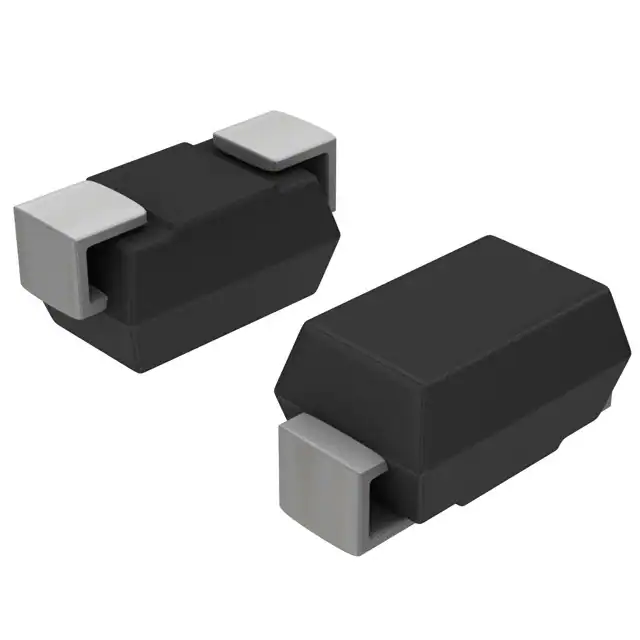
- Part No.:
- P4SMA75CA
- Manufacturer:
- Taiwan Semiconductor Corporation
- Category:
- TVS Diodes
- Package:
- DO-214AC, SMA
- Datasheet:
-
 P4SMA75CA.pdf
- Description:
- TVS DIODE 64.1VWM 103VC DO214AC
- Quantity:
- Payment:

- Shipping:

Inventory:7,047
Please send an inquiry. Send us your inquiry, and we will respond immediately.
Product details
Overview
P4SMA75CA from Taiwan Semiconductor is a bidirectional surface-mount transient voltage suppressor (TVS) diode in DO-214AC (SMA) package, designed for robust ESD and surge protection in DC power rails. It features a 67.5–82.5 V breakdown voltage (VBR), 60.7 V working stand-off voltage (VWM), 103 V clamping voltage (VC) at 4.0 A peak impulse current, and 400 W peak pulse power rating per 10/1000 µs waveform - deployed in automotive body electronics and industrial DC/DC converters.
For engineers reviewing the P4SMA75CA datasheet, P4SMA75CA pinout, P4SMA75CA application, or P4SMA75CA equivalent, key selection criteria include bidirectional clamping capability, ISO 7637-2 Pulse 1/2a/2b/3a/3b compliance, <1 µA reverse leakage at VWM, -55°C to +150°C operating junction temperature, and DO-214AC mechanical compatibility with automated SMT assembly.
Technical Context
The P4SMA75CA implements a glass-passivated silicon junction optimized for fast transient response (<1.0 ps typical) and low capacitance, enabling effective suppression of high-speed voltage spikes without signal distortion. Its bidirectional configuration ensures symmetrical clamping in both polarities, eliminating need for polarity-aware placement in AC-coupled or floating-rail systems.
It operates within a 150°C maximum junction temperature limit and supports repetitive surge events only when derated per Fig.2 of the datasheet; non-repetitive 400 W pulse handling follows the standardized 10/1000 µs double-exponential waveform defined in ANSI/IEEE C62.35.
Key Specifications
| Parameter | Value and Actual Design Meaning |
|---|---|
| VBR min/max | 67.5 V / 82.5 V at 1.0 mA test current - defines reliable conduction onset window under surge conditions |
| VWM | 60.7 V - maximum continuous DC or RMS voltage the device blocks without significant leakage |
| VC @ IPPM | 103 V at 4.0 A (10/1000 µs) - peak clamped voltage seen by protected circuit during worst-case surge |
| PPPM | 400 W - maximum single-pulse transient energy absorption capability |
| IR @ VWM | <1 µA - ensures negligible standby power loss and minimal loading on sensitive voltage rails |
| TJ range | -55°C to +150°C - supports operation in under-hood automotive and industrial ambient environments |
| Configuration | Bidirectional - provides symmetrical overvoltage protection without polarity dependency |
Pinout & Package
Package: DO-214AC (SMA), surface-mount, molded plastic case with matte tin-plated leads; polarity indicated by cathode band (bidirectional operation renders band non-functional but retained for marking consistency).
| Pin/Terminal | Circuit Role | Design Meaning |
|---|---|---|
| Anode/Cathode (marked band) | Transient current path terminal | Provides low-impedance shunt path to ground or rail during overvoltage; bidirectional symmetry means either terminal serves as anode or cathode depending on polarity of transient |
| Case / Body | Non-electrical mechanical interface | No electrical connection; serves only as thermal and mechanical mounting structure per JEDEC DO-214AC standard |
Key Features
| Feature | Design Value |
|---|---|
| Glass passivated junction | Ensures stable VBR tolerance and long-term reliability under thermal cycling and humidity stress |
| ISO 7637-2 compliance | Validated for automotive load-dump and inductive-switching transients (Pulse 1/2a/2b/3a/3b) |
| Moisture sensitivity level 1 | Enables unlimited floor life before reflow; no baking required prior to SMT assembly |
| RoHS & halogen-free | Meets IEC 61249-2-21 and EU RoHS Directive 2011/65/EU for environmentally constrained designs |
| Fast response time | <1.0 ps typical - clamps transients before downstream ICs experience damaging overvoltage |
Applications
| Automotive Body Control Module (BCM) | Industrial DC/DC Converter Input Stage |
|---|---|
Use Scenario: Protects microcontroller I/O and CAN transceiver power rails from load dump and alternator ripple in 12 V vehicle systems. IC Role / Device Role: Bidirectional TVS placed between VBAT and GND to clamp negative-going spikes and positive surges symmetrically. Use Value: Maintains system uptime by limiting voltage excursions to ≤103 V during 400 W transients, preventing latch-up or gate oxide damage in 3.3 V/5 V logic. | Use Scenario: Shields primary-side MOSFET gate drivers and controller ICs from switching-induced voltage overshoot in isolated flyback converters. IC Role / Device Role: Transient suppressor across input bulk capacitor terminals to absorb reflected energy from transformer leakage inductance. Use Value: Enables use of lower-voltage-rated (e.g., 100 V) MOSFETs by clamping input rail spikes to 103 V, reducing BOM cost and footprint. |
| LED Driver Power Supply | Smart Meter Power Input Protection |
Use Scenario: Safeguards constant-current LED driver ICs against lightning-induced surges on AC-DC adapter outputs. IC Role / Device Role: Secondary-side TVS on low-voltage DC output rail (e.g., 24 V) to protect LED string controllers from line-to-rail transients. Use Value: Prevents catastrophic failure of LED driver ICs by limiting clamped voltage to 103 V while maintaining <1 µA leakage at nominal 24 V operation. | Use Scenario: Secures metering SoC power inputs against EFT bursts and surge events per IEC 61000-4-4/5 in utility-grade smart meters. IC Role / Device Role: First-line transient suppressor on 3.3 V or 5 V supply rail entering metrology ASIC or communication module. Use Value: Delivers sub-1 µA leakage and 103 V clamping to preserve accuracy of precision ADC references and avoid false resets during EMC testing. |
Equivalent & Alternatives
The following parts are listed as comparable options for similar transient voltage suppression applications.
| Alternative Part | Technical Difference | Application Difference | Selection Advice |
|---|---|---|---|
| SMBJ75CA (Bourns) | Same DO-214AA package; 400 W rating; VBR = 75.6–83.6 V; VC = 121 V @ 3.3 A - higher clamping voltage, lower peak current | Less effective clamping margin for 75 V nominal rails due to 121 V VC; suitable where layout allows higher VC tolerance | Select P4SMA75CA when tighter clamping (103 V) and higher IPPM (4.0 A) are required for critical 75 V rail protection |
| 1.5SMC75CA (ON Semiconductor) | DO-214AB (SMC) package; 1500 W rating; VBR = 71.3–78.8 V; VC = 121 V @ 12.4 A - larger footprint, higher power, same VC | Requires PCB area increase; used where multi-kW surge immunity is mandated (e.g., telecom central office) | Choose P4SMA75CA for space-constrained SMT designs needing 400 W protection in minimal DO-214AC footprint |
Compared with SMBJ75CA and 1.5SMC75CA, the P4SMA75CA delivers superior clamping performance (103 V vs. 121 V) in the smallest surface-mount package, making it optimal for high-density automotive and industrial PCBs where voltage margin and board space are critical.
Availability
P4SMA75CA is available at Aetrix Electronics and suitable for automotive body electronics, industrial DC/DC converters, LED driver power supplies, and smart meter power input protection requiring stable component supply and full traceability.
Supply support for P4SMA75CA includes scheduled delivery planning, volume procurement assistance, BOM continuity management, traceable sourcing, and lifecycle availability coordination for OEM customers, industrial embedded developers, connected-device designers, and electronics production programs.
Manufacturer
Taiwan Semiconductor Company (TSC) is a vertically integrated Taiwanese semiconductor manufacturer specializing in discrete power devices, TVS diodes, rectifiers, and MOSFETs for automotive, industrial, and consumer markets.
The P4SMA75CA belongs to TSC's P4SMAx(A) family of surface-mount TVS diodes engineered specifically for ISO 7637-2-compliant automotive and harsh-environment industrial surge protection with high reliability and automated assembly compatibility.
FAQ
What is the clamping voltage of the P4SMA75CA under standard 10/1000 µs surge conditions?
The P4SMA75CA has a maximum clamping voltage (VC) of 103 V when subjected to its rated peak pulse current of 4.0 A using the 10/1000 µs waveform. This value is measured per ANSI/IEEE C62.35 and represents the upper voltage limit imposed on the protected circuit during transient events - critical for ensuring downstream ICs remain within absolute maximum ratings. The P4SMA75CA achieves this with tight VBR tolerance (67.5–82.5 V) and low dynamic impedance.
Is the P4SMA75CA unidirectional or bidirectional, and how does that affect circuit placement?
The P4SMA75CA is a bidirectional TVS diode, indicated by the "CA" suffix, meaning it provides symmetrical clamping for both positive and negative transients without polarity sensitivity. Unlike unidirectional variants (e.g., P4SMA75A), no orientation alignment is required during placement - the cathode band marking is retained for consistency but carries no functional significance. This simplifies layout and eliminates risk of misorientation in floating or AC-coupled rails. The P4SMA75CA thus supports robust protection in differential signaling paths and dual-rail systems.
Does the P4SMA75CA meet automotive surge immunity standards such as ISO 7637-2?
Yes, the P4SMA75CA is explicitly rated to meet ISO 7637-2 requirements for Pulse 1 (inductive load disconnect), Pulse 2a (sudden load removal), Pulse 2b (supply interruption), Pulse 3a (capacitive coupled noise), and Pulse 3b (power line noise). This validation is documented in Taiwan Semiconductor's official datasheet (Version S2102) and confirms suitability for 12 V and 24 V automotive subsystems including body control modules, infotainment power supplies, and sensor interfaces. The P4SMA75CA's 400 W rating and 103 V clamping directly address the energy and voltage limits specified in those pulses.
What is the maximum operating junction temperature for the P4SMA75CA, and how does it impact thermal design?
The P4SMA75CA has a maximum junction temperature (TJ) of +150°C, with a specified operating range from -55°C to +150°C. This rating enables deployment in under-hood automotive locations and industrial enclosures without active cooling. However, its 400 W peak pulse power must be derated above 25°C ambient per Figure 2 in the datasheet - at 100°C ambient, usable pulse power drops to ~240 W. Thermal design must therefore consider PCB copper area, adjacent heat sources, and pulse repetition rate to avoid exceeding TJ max. The P4SMA75CA's DO-214AC package relies on pad thermal mass for transient dissipation, not continuous conduction.
How does the P4SMA75CA compare to the P4SMA75A in terms of electrical performance and application use?
The P4SMA75CA is the bidirectional version, while P4SMA75A is unidirectional. Key differences include identical VBR (71.3–78.8 V), VWM (64.1 V), and VC (103 V), but P4SMA75CA clamps symmetrically in both directions - essential for AC lines, differential buses, or floating grounds. P4SMA75A requires correct cathode orientation and only protects against positive transients relative to ground. The P4SMA75CA eliminates orientation errors and supports broader use cases like CAN bus protection or dual-supply rail clamping, whereas P4SMA75A suits simpler DC rail-to-ground protection where polarity is fixed.
P4SMA75CA Specifications
- Product attributes
- Attribute value
- Manufacturer:
- Taiwan Semiconductor Corporation
- Package/Case:
- DO-214AC, SMA
- Series:
- P4SMA
- Packaging:
- Tape & Reel (TR)
- Product Status:
- Active
- Type:
- Zener
- Unidirectional Channels:
- -
- Bidirectional Channels:
- 1
- Voltage - Reverse Standoff (Typ):
- 64.1V
- Voltage - Breakdown (Min):
- 71.3V
- Voltage - Clamping (Max) @ Ipp:
- 103V
- Current - Peak Pulse (10/1000µs):
- 4A
- Power - Peak Pulse:
- 400W
- Power Line Protection:
- No
- Applications:
- General Purpose
- Capacitance @ Frequency:
- -
- Operating Temperature:
- -55°C ~ 150°C (TJ)
- Grade:
- -
- Qualification:
- -
- Mounting Type:
- Surface Mount
- Supplier Device Package:
- DO-214AC (SMA)
P4SMA75CA FAQ
1.How can I place an order for P4SMA75CA through Aetrix?
Please submit a Request for Quotation (RFQ) for P4SMA75CA on Aetrix. Our sales agent will provide a competitive quotation and guide you through the order confirmation once you accept the terms.
2.Are the price and stock information for P4SMA75CA reliable?
The price and inventory of P4SMA75CA are updated periodically and may fluctuate due to market conditions. Stock and pricing data are typically refreshed every 24 hours. Quotation validity for P4SMA75CA is usually 5 days.
3.What payment methods are accepted for P4SMA75CA?
We accept Wire Transfer, PayPal, Credit Card, Western Union, MoneyGram, and Escrow for P4SMA75CA transactions.
Note: Certain payment methods may incur a processing fee.
4.How is shipping managed for P4SMA75CA?
P4SMA75CA orders can be shipped via leading logistics carriers, including DHL, UPS, FedEx, TNT, or Registered Mail.
Once your P4SMA75CA order is processed, you will receive an email with the shipment details and tracking number.
Note: Tracking information may take up to 24 hours to appear. Express delivery typically takes 3–5 business days.
5.How can I obtain technical support or documentation for P4SMA75CA?
For technical support, including P4SMA75CA datasheets, pinout diagrams, or application guidance, please contact our engineering support team. They can provide detailed documentation and assistance for your P4SMA75CA requirements.
6.How does Aetrix verify that P4SMA75CA is sourced from the original manufacturer or authorized distributors?
All P4SMA75CA products on Aetrix are procured from qualified distributors and authorized channels. Our dedicated quality assurance team conducts strict verification, including traceability checks and, if necessary, third-party testing. This ensures that P4SMA75CA meets industry standards.
7.What is the process for return or replacement of P4SMA75CA?
All P4SMA75CA units undergo pre-shipment inspection (PSI). If there is an issue with P4SMA75CA, returns or replacements are accepted under the following conditions:
1.Quantity discrepancies, incorrect items, or visible external defects (such as breakage or corrosion), acknowledged by Aetrix.
2.The issue is reported within 90 days of delivery.
3.The P4SMA75CA part is unused and in its original packaging.
Return procedure for P4SMA75CA:
1.Submit a request within 90 days.
2.Obtain a Return Material Authorization (RMA) from Aetrix.
P4SMA75CA Tags
-
ESD9B5.0ST5G
onsemi
-
DESD3V3E1BL-7B
Diodes Incorporated
-
ESD5Z3.3T1G
onsemi
-
D5V0H1B2LP-7B
Diodes Incorporated
-
D5V0P1B2LP-7B
Diodes Incorporated
-
DESD5V0U1BA-7
Diodes Incorporated
-
ESD5Z5.0T1G
onsemi
-
DESD5V0U1BB-7
Diodes Incorporated
-
D12V0L1B2LP-7B
Diodes Incorporated
-
PESD2V0Y1BSFYL
Nexperia USA Inc.
-
DF2S5M4CT,L3F
Toshiba Semiconductor and Storage
-
D5V0L1B2WS-7
Diodes Incorporated
Tech Hub

Counterfeit components can hide behind convincing markings and passing basic function tests. This engineering reference covers source traceability, external inspection, X-ray, XRF, electrical testing, …

A practical engineering and sourcing framework covering lifecycle verification, lifetime-buy calculations, replacement qualification, supplier checks and counterfeit-risk controls.

TTL and CMOS logic families differ in thresholds, loading, output drive, power and timing. This engineering guide compares 74HC and 74HCT, calculates noise margins and checks 3.3 V/5 V compatibility.

A practical engineering guide to 3.3V and 5V logic compatibility, input thresholds, resistor dividers, translator ICs, MOSFET level shifting, I2C pull-ups, timing limits and power-sequencing risks.

The 74HC595 uses push-pull logic outputs, while the TPIC6B595 uses 50 V open-drain DMOS sinks for higher-power loads. This guide compares timing, current limits, 3.3 V interfacing, load wiring, thermal…

The 74HC595 converts serial data into eight stable parallel outputs. This guide covers pin functions, shift and storage timing, OE and MR behavior, drive-current limits, cascading, voltage compatibilit…

A technical comparison of level-sensitive latches and edge-triggered flip-flops, covering timing windows, setup and hold limits, master–slave operation, time borrowing, race-through, HDL inference and…

A D latch stores one bit while Enable controls when data can pass. This reference covers gate-level operation, truth tables, transparency, setup and hold timing, LE versus OE, common ICs and practical …

An SR latch stores one bit through cross-coupled feedback. This engineering reference covers NOR and NAND implementations, truth tables, forbidden-state recovery, gated operation, switch debouncing, fa…

Latch circuits retain one bit through feedback. This technical reference covers SR and D latches, truth tables, transparency, timing limits, latch-versus-flip-flop behavior, applications and common log…


