
 My Inquiry
 My Account


Nexperia USA Inc. PESD1IVN27-UX
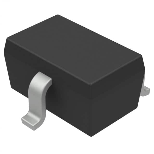
- Part No.:
- PESD1IVN27-UX
- Manufacturer:
- Nexperia USA Inc.
- Category:
- TVS Diodes
- Package:
- SC-70, SOT-323
- Datasheet:
-
 PESD1IVN27-UX.pdf
- Description:
- TVS DIODE 27VWM 45VC SOT323
- Quantity:
- Payment:

- Shipping:

Inventory:885
Please send an inquiry. Send us your inquiry, and we will respond immediately.
Product details
Overview
PESD1IVN27-UX from Nexperia is a bidirectional automotive-grade ESD protection diode in SOT323 (SC-70) package, designed for transient suppression on in-vehicle network lines. It delivers 27 V reverse standoff voltage, 36 V clamping voltage at 3 A, 30 kV IEC 61000-4-2 ESD immunity, <1 nA leakage, and 14–17 pF capacitance - enabling robust CAN, LIN, FlexRay, and SENT bus line protection in harsh automotive environments.
For engineers reviewing the PESD1IVN27-UX datasheet, PESD1IVN27-UX pinout, PESD1IVN27-UX application, or PESD1IVN27-UX equivalent, this device is selected for high-reliability IVN bus protection where low clamping, ultra-low leakage, and AEC-Q101 qualification are mandatory - especially when designing against ISO 10605 (330 pF/330 Ω) and ISO 7637-3 pulse stress.
Technical Context
This dual-cathode TVS diode implements a symmetrical bidirectional clamping architecture with two independent ESD protection paths sharing a common anode (Pin 2, n.c.). Its VBR of 28–38 V at 10 mA and dynamic resistance of 0.2 Ω (TLP, 10 A) ensure fast response and minimal voltage overshoot during ±8 kV contact discharge events.
The device operates across –55 °C to +150 °C ambient, supports peak pulse current up to 3 A (8/20 μs), and maintains stable clamping performance under junction temperatures up to 150 °C - validated per AEC-Q101 stress tests including temperature cycling, HTRB, and ESD robustness.
Key Specifications
| Parameter | Value and Actual Design Meaning |
|---|---|
| Reverse Standoff Voltage | 27 V - maximum continuous operating voltage before conduction begins; sets safe margin above 24 V automotive supply rails. |
| Clamping Voltage | 36 V (typ.) at 3 A - limits transient voltage seen by downstream transceivers during ISO 10605 or IEC 61000-4-2 events. |
| ESD Withstand | ±30 kV (IEC 61000-4-2 & ISO 10605 C = 330 pF/R = 330 Ω) - exceeds automotive OEM requirements for connector-level ESD immunity. |
| Diode Capacitance | 14–17 pF at 0 V - low enough to avoid signal integrity degradation on high-speed IVN buses (e.g., FlexRay up to 10 Mbps). |
| Leakage Current | <1 nA at 27 V - prevents parasitic loading and battery drain in always-on vehicle networks. |
| Peak Pulse Current | 3 A (8/20 μs) - handles ISO 7637-3 Pulse b (+100 V) and Pulse a (–150 V) surge transients without failure. |
| Package | SOT323 (SC-70) - 2.0 × 1.25 × 0.95 mm surface-mount footprint compatible with automated reflow assembly and space-constrained ECUs. |
Pinout & Package
SOT323 (SC-70) plastic surface-mount package: 3-terminal, 1.3 mm pitch, 2.0 mm × 1.25 mm × 0.95 mm body size, optimized for high-density PCB layouts near connectors.
| Pin/Terminal | Circuit Role | Design Meaning |
|---|---|---|
| 1 | Cathode (Diode 1) | Connects to protected IVN line (e.g., LIN or CAN_H); forms one half of bidirectional clamping path. |
| 2 | Not Connected | Internal floating terminal - must remain unconnected on PCB; no routing or soldering allowed. |
| 3 | Cathode (Diode 2) | Connects to same protected IVN line as Pin 1; enables symmetrical ± clamping relative to ground reference. |
Key Features
| Feature | Design Value |
|---|---|
| Bidirectional Clamping | Enables single-device protection of differential or single-ended IVN signals without polarity constraints - e.g., LIN bus referenced to chassis ground. |
| AEC-Q101 Qualified | Validated for automotive Grade 3 (–40 °C to +125 °C case temp) operation, including HTGB, TC, and ESD stress - suitable for engine bay and infotainment modules. |
| Ultra-Low Capacitance | 14–17 pF ensures minimal signal distortion on 1–10 Mbps IVN protocols, preserving rise/fall times and eye diagram integrity. |
| Sub-1 nA Leakage | Eliminates measurable current draw in sleep-mode vehicle networks, supporting >10-year battery life in always-on telematics nodes. |
| ISO 7637-3 Compliance | Withstands –150 V (Pulse a) and +100 V (Pulse b) load-dump and alternator-switching transients - critical for 12 V/24 V power domain coupling. |
Applications
| Automotive LIN Bus Protection | Automotive CAN Bus Protection |
|---|---|
Use Scenario: Protecting LIN slave nodes (e.g., door modules, seat controllers) from ESD events at external connectors exposed to human touch. IC Role / Device Role / Timing Role: Bidirectional transient voltage suppressor placed directly at LIN header, shunting ESD energy to chassis ground before reaching transceiver input. Use Value: Prevents latch-up or permanent damage to LIN transceivers (e.g., TJA1020) while maintaining <15 ns response time and sub-36 V clamping. |
Use Scenario: Safeguarding high-speed CAN FD interfaces in ADAS ECUs against connector-level ESD and coupled surges from adjacent power circuits. IC Role / Device Role / Timing Role: Low-capacitance TVS pair protecting CAN_H/CAN_L differential pair, referenced to ground via shared cathodes. Use Value: Maintains CAN signal integrity up to 5 Mbps with ≤17 pF loading and clamps ±8 kV discharges to <45 V - within ISO 11898-2 receiver tolerance. |
| FlexRay Bus Protection | SENT Sensor Interface Protection |
Use Scenario: Shielding FlexRay physical layer (e.g., TJA1080A) in x-by-wire systems from ESD during service or manufacturing handling. IC Role / Device Role / Timing Role: Symmetrical clamping device installed at FlexRay connector, minimizing stub length to preserve 10 Mbps signal fidelity. Use Value: Delivers 36 V clamping at 3 A with 0.2 Ω dynamic resistance - limiting overshoot to <1.5 V above VRWM during fast transients. |
Use Scenario: Securing SENT (Single Edge Nibble Transmission) sensor links (e.g., pressure, temperature) in powertrain control units against ESD-induced bit errors. IC Role / Device Role / Timing Role: Low-leakage TVS on SENT signal line, placed between sensor harness connector and microcontroller GPIO input. Use Value: Enables reliable 125 kbps SENT communication with <1 nA leakage - avoiding false edge detection or baseline shift in analog front-end circuits. |
Equivalent & Alternatives
The following parts are listed as comparable options for similar bidirectional automotive ESD protection applications.
| Alternative Part | Technical Difference | Application Difference | Selection Advice |
|---|---|---|---|
| ON Semiconductor SZ1.5SMC27A | Unidirectional, higher clamping (53 V at 36.7 A), larger SMC package (7.1 × 6.2 mm), 1000 W peak power. | Requires dual-device layout for bidirectional protection; suited for high-energy 12 V power line surge, not IVN signal lines. | Select only if protecting non-differential power rails with >100 A surge capability - not recommended for CAN/LIN/FlexRay signal integrity. |
| Vishay DEH12M27 | Bidirectional, 27 V VRWM, 40 V VCL at 3 A, 20 pF capacitance, AEC-Q101 qualified, SOD-323 package. | Higher capacitance increases signal attenuation on >5 Mbps FlexRay; slightly slower response due to larger junction area. | Acceptable for LIN and low-speed CAN (≤125 kbps), but PESD1IVN27-UX preferred for high-speed IVN due to lower Cd and tighter VCL distribution. |
Compared with SZ1.5SMC27A and DEH12M27, PESD1IVN27-UX offers superior signal integrity for high-speed IVN buses via its 14–17 pF capacitance and 36 V clamping, while maintaining AEC-Q101 compliance in the smallest footprint - making it optimal for space-constrained ECU designs requiring precise transient control.
Availability
PESD1IVN27-UX is available at Aetrix Electronics and suitable for automotive electronic control units, in-vehicle networking subsystems, and sensor interface modules requiring stable component supply across extended temperature ranges and long production lifecycles.
Supply support for PESD1IVN27-UX includes scheduled delivery planning, volume procurement assistance, BOM continuity management, traceable sourcing, and lifecycle availability coordination for OEM customers, industrial embedded developers, connected-device designers, and electronics production programs.
Manufacturer
Nexperia is a global semiconductor expert focused on high-volume, high-reliability logic, discrete, and MOSFET solutions - with leadership in automotive-qualified components and advanced packaging technologies.
This device belongs to Nexperia's Automotive ESD Protection portfolio, engineered specifically for robust transient suppression on in-vehicle network buses - balancing low capacitance, tight clamping, and AEC-Q101 reliability for next-generation ECU architectures.
FAQ
What is the function of Pin 2 (n.c.) on the PESD1IVN27-UX?
Pin 2 is internally not connected and must remain unattached on the PCB. It serves no electrical function and is a structural artifact of the SOT323 leadframe design. Routing or soldering to Pin 2 risks mechanical stress, thermal mismatch, or unintended coupling - violating Nexperia's layout guidelines and potentially degrading ESD performance.
Can PESD1IVN27-UX protect both CAN_H and CAN_L simultaneously?
No - PESD1IVN27-UX protects a single signal line (e.g., CAN_H or CAN_L) using its dual-cathode configuration referenced to ground. For full differential CAN bus protection, two devices are required: one per line. Its symmetrical clamping enables identical protection on either line without polarity concerns.
How does the 0.2 Ω dynamic resistance impact system-level ESD performance?
A dynamic resistance of 0.2 Ω (measured at 10 A TLP) minimizes voltage overshoot during fast ESD events by reducing IR drop across the device. This ensures clamping stays within 36–45 V even under high di/dt conditions - critical for preventing damage to sensitive transceivers like the TJA1042 or MCP2562.
Is PESD1IVN27-UX compatible with lead-free reflow profiles?
Yes - the SOT323 package is qualified for standard lead-free reflow per JEDEC J-STD-020, with peak temperatures up to 260 °C. The recommended footprint (Fig. 14) uses 0.55 mm solder paste stencil openings and 1.325 mm pad width to ensure reliable wetting and void-free joints without tombstoning.
PESD1IVN27-UX Specifications
- Product attributes
- Attribute value
- Manufacturer:
- Nexperia USA Inc.
- Package/Case:
- SC-70, SOT-323
- Series:
- -
- Packaging:
- Tape & Reel (TR)
- Product Status:
- Active
- Type:
- Zener
- Unidirectional Channels:
- -
- Bidirectional Channels:
- 1
- Voltage - Reverse Standoff (Typ):
- 27V
- Voltage - Breakdown (Min):
- 28V
- Voltage - Clamping (Max) @ Ipp:
- 45V
- Current - Peak Pulse (10/1000µs):
- 3A (8/20µs)
- Power - Peak Pulse:
- -
- Power Line Protection:
- No
- Applications:
- CAN
- Capacitance @ Frequency:
- 14pF @ 1MHz
- Operating Temperature:
- -55°C ~ 150°C (TA)
- Grade:
- Automotive
- Qualification:
- AEC-Q101
- Mounting Type:
- Surface Mount
- Supplier Device Package:
- SOT-323
PESD1IVN27-UX FAQ
1.How can I place an order for PESD1IVN27-UX through Aetrix?
Please submit a Request for Quotation (RFQ) for PESD1IVN27-UX on Aetrix. Our sales agent will provide a competitive quotation and guide you through the order confirmation once you accept the terms.
2.Are the price and stock information for PESD1IVN27-UX reliable?
The price and inventory of PESD1IVN27-UX are updated periodically and may fluctuate due to market conditions. Stock and pricing data are typically refreshed every 24 hours. Quotation validity for PESD1IVN27-UX is usually 5 days.
3.What payment methods are accepted for PESD1IVN27-UX?
We accept Wire Transfer, PayPal, Credit Card, Western Union, MoneyGram, and Escrow for PESD1IVN27-UX transactions.
Note: Certain payment methods may incur a processing fee.
4.How is shipping managed for PESD1IVN27-UX?
PESD1IVN27-UX orders can be shipped via leading logistics carriers, including DHL, UPS, FedEx, TNT, or Registered Mail.
Once your PESD1IVN27-UX order is processed, you will receive an email with the shipment details and tracking number.
Note: Tracking information may take up to 24 hours to appear. Express delivery typically takes 3–5 business days.
5.How can I obtain technical support or documentation for PESD1IVN27-UX?
For technical support, including PESD1IVN27-UX datasheets, pinout diagrams, or application guidance, please contact our engineering support team. They can provide detailed documentation and assistance for your PESD1IVN27-UX requirements.
6.How does Aetrix verify that PESD1IVN27-UX is sourced from the original manufacturer or authorized distributors?
All PESD1IVN27-UX products on Aetrix are procured from qualified distributors and authorized channels. Our dedicated quality assurance team conducts strict verification, including traceability checks and, if necessary, third-party testing. This ensures that PESD1IVN27-UX meets industry standards.
7.What is the process for return or replacement of PESD1IVN27-UX?
All PESD1IVN27-UX units undergo pre-shipment inspection (PSI). If there is an issue with PESD1IVN27-UX, returns or replacements are accepted under the following conditions:
1.Quantity discrepancies, incorrect items, or visible external defects (such as breakage or corrosion), acknowledged by Aetrix.
2.The issue is reported within 90 days of delivery.
3.The PESD1IVN27-UX part is unused and in its original packaging.
Return procedure for PESD1IVN27-UX:
1.Submit a request within 90 days.
2.Obtain a Return Material Authorization (RMA) from Aetrix.
PESD1IVN27-UX Tags
-
ESD9B5.0ST5G
onsemi
-
DESD3V3E1BL-7B
Diodes Incorporated
-
ESD5Z3.3T1G
onsemi
-
D5V0H1B2LP-7B
Diodes Incorporated
-
D5V0P1B2LP-7B
Diodes Incorporated
-
DESD5V0U1BA-7
Diodes Incorporated
-
ESD5Z5.0T1G
onsemi
-
DESD5V0U1BB-7
Diodes Incorporated
-
D12V0L1B2LP-7B
Diodes Incorporated
-
PESD2V0Y1BSFYL
Nexperia USA Inc.
-
DF2S5M4CT,L3F
Toshiba Semiconductor and Storage
-
D5V0L1B2WS-7
Diodes Incorporated
Tech Hub

A practical engineering and sourcing framework covering lifecycle verification, lifetime-buy calculations, replacement qualification, supplier checks and counterfeit-risk controls.

TTL and CMOS logic families differ in thresholds, loading, output drive, power and timing. This engineering guide compares 74HC and 74HCT, calculates noise margins and checks 3.3 V/5 V compatibility.

A practical engineering guide to 3.3V and 5V logic compatibility, input thresholds, resistor dividers, translator ICs, MOSFET level shifting, I2C pull-ups, timing limits and power-sequencing risks.

The 74HC595 uses push-pull logic outputs, while the TPIC6B595 uses 50 V open-drain DMOS sinks for higher-power loads. This guide compares timing, current limits, 3.3 V interfacing, load wiring, thermal…

The 74HC595 converts serial data into eight stable parallel outputs. This guide covers pin functions, shift and storage timing, OE and MR behavior, drive-current limits, cascading, voltage compatibilit…

A technical comparison of level-sensitive latches and edge-triggered flip-flops, covering timing windows, setup and hold limits, master–slave operation, time borrowing, race-through, HDL inference and…

A D latch stores one bit while Enable controls when data can pass. This reference covers gate-level operation, truth tables, transparency, setup and hold timing, LE versus OE, common ICs and practical …

An SR latch stores one bit through cross-coupled feedback. This engineering reference covers NOR and NAND implementations, truth tables, forbidden-state recovery, gated operation, switch debouncing, fa…

Latch circuits retain one bit through feedback. This technical reference covers SR and D latches, truth tables, transparency, timing limits, latch-versus-flip-flop behavior, applications and common log…

An engineering guide to LED driver operation, constant-current and constant-voltage outputs, linear and switching topologies, dimming, IC selection, calculations, replacement compatibility, and fault c…


