
 My Inquiry
 My Account


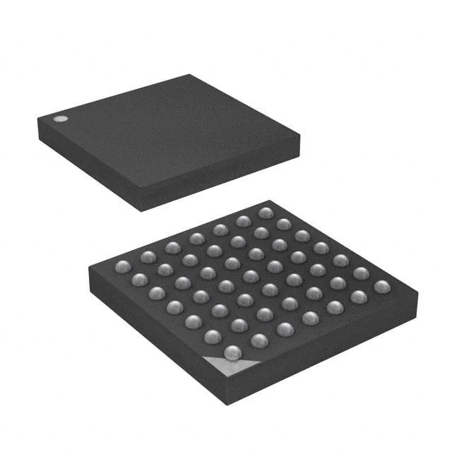
NXP Semiconductors PN7120A0EV/C10801E
- Part No.:
- PN7120A0EV/C10801E
- Manufacturer:
- NXP Semiconductors
- Category:
- RFID, RF Access, Monitoring ICs
- Package:
- 49-VFBGA
- Datasheet:
-
 PN7120A0EV/C10801E.pdf
- Description:
- IC RFID READER 13.56MHZ 49VFBGA
- Quantity:
- Payment:

- Shipping:

Inventory:4,718
Please send an inquiry. Send us your inquiry, and we will respond immediately.
Product details
Overview
PN7120A0EV/C10801E from NXP Semiconductors is an NFC controller IC with embedded ARM Cortex-M0 core and integrated firmware, supporting all NFC Forum modes (Reader/Writer, Card Emulation, P2P) at 13.56 MHz. It features I²C host interface (up to 3.4 MBaud), ultra-low-power polling loop (150 μA typical), and direct battery operation (2.3–5.5 V). It is designed for rapid integration into Linux/Android systems requiring compact, low-BOM NFC functionality.
For engineers reviewing the PN7120A0EV/C10801E datasheet, PN7120A0EV/C10801E pinout, PN7120A0EV/C10801E application, or PN7120A0EV/C10801E equivalent, key selection considerations include its NCI 1.0 compliance, integrated RF front-end for small-form-factor antennas, autonomous polling loop execution, and support for ISO/IEC 14443-A/B, FeliCa, MIFARE Classic/DESFire, and ISO/IEC 15693 protocols.
Technical Context
The PN7120A0EV/C10801E implements a full NCI 1.0-compliant host interface over I²C, with programmable slave address (0x50/0x51 or 0x52/0x53) and clock-stretching support. Its ARM Cortex-M0 executes pre-integrated firmware that handles real-time NFC protocol stack, polling loop sequencing, and device discovery without host CPU intervention.
Its RF architecture combines a highly integrated demodulator/decoder, buffered antenna drivers (TX1/TX2), internal RF level detector, and dual-clock system (27.12 MHz crystal or PLL-synthesized reference + 380 kHz LFO for low-power timing). Power management includes Hard Power Down, Standby, Monitor, and Active states - enabling sub-μA wake-up via RF field, timer, or I²C activity.
Key Specifications
| Parameter | Value and Actual Design Meaning |
|---|---|
| Host Interface | I²C-bus slave, up to 3.4 MBaud; supports Standard/Fast/High-speed modes with clock stretching |
| RF Protocols | Fully supports NFCIP-1/NFCIP-2, ISO/IEC 14443-A/B, ISO/IEC 15693, FeliCa, MIFARE Classic 1K/4K, DESFire, Ultralight, Jewel |
| Supply Voltage Range | VBAT: 2.3–5.5 V (Card Emulation) or 2.7–5.5 V (Reader/Active); VDD(PAD): 1.65–1.95 V (1.8 V host) or 3.0–3.6 V (3.3 V host) |
| Low-Power Polling Current | 150 μA typical at 500 ms loop time, enabling multi-week battery life in portable devices |
| Power States | Hard Power Down (10 μA), Standby (≤20 μA), Monitor (≤12 μA), Active (170 mA max in PCD mode) |
| Antenna Interface | Dual differential TX outputs (TX1/TX2), ANT1/ANT2 listen-mode connections, integrated RF level detector |
| Crystal Requirement | 27.12 MHz ±100 ppm (FCC), ±50 ppm (ISO/IEC), 10 pF load capacitance, ≤100 Ω ESR |
Pinout & Package
VFBGA49 package (SOT1320-1), 4.0 × 4.0 × 0.5 mm, 0.4 mm pitch, bottom-side ball layout.
| Pin/Terminal | Circuit Role | Design Meaning |
|---|---|---|
| IRQ | Interrupt request output | Active-low signal notifying host of card detection, P2P event, or firmware completion |
| VEN | Reset / Hard Power Down control | Low-level assertion (<0.4 V) forces Hard Power Down; high-level enables full operation |
| I2CSCL / I2CSDA / I2CADR0 | I²C host interface signals | Configurable 7-bit slave address (0x50/0x51 or 0x52/0x53); supports clock stretching for flow control |
| TX1 / TX2 / ANT1 / ANT2 | RF antenna interface | Differential transmitter outputs and listen-mode antenna terminals; require external matching network |
| VBAT / VBAT1 / VBAT2 | Battery supply inputs | All three must be connected to same 2.3–5.5 V battery rail; enable direct battery-powered operation |
| VDD(TX) | Transmitter LDO output | Provides decoupled 3.3 V supply to antenna driver stage; current-limited to 180 mA for protection |
Key Features
| Feature | Design Value |
|---|---|
| Integrated NCI 1.0 firmware stack | Eliminates need for host-side NFC protocol implementation; reduces Android/Linux integration effort to <5 API calls |
| Autonomous polling loop | Executes ISO/IEC 14443-A/B, FeliCa, ISO/IEC 15693, and NFC Forum Tag Type 1–4 discovery sequences without host CPU involvement |
| Ultra-low-power monitoring | 12 μA Standby current with RF-field wake-up capability enables always-on NFC presence detection in battery-constrained wearables |
| Single-supply battery operation | Direct 2.3–5.5 V battery input with integrated PMU eliminates need for external DC-DC or LDO regulators |
| Small-form-factor antenna support | High-sensitivity RF front-end and active load modulation enable functional NFC with antennas as small as 25 mm² |
Applications
| Smart Home Gateways | Wearable Health Monitors |
|---|---|
Use Scenario: NFC-enabled home automation hub pairing with locks, sensors, and lighting controllers via tap-to-configure. IC Role / Device Role / Timing Role: Acts as NFC Reader/Writer and P2P Initiator to exchange provisioning data and firmware updates with peripheral devices. Use Value: Enables zero-configuration onboarding using standardized NFC Forum T4T platform, reducing user setup time from minutes to seconds. | Use Scenario: Fitness tracker initiating secure health-data transfer to smartphone upon tap. IC Role / Device Role / Timing Role: Functions as NFC Target (Card Emulation) with MIFARE DESFire EV2 profile for encrypted data exchange. Use Value: Delivers sub-150 μA average current during polling, extending battery life to >7 days between charges while maintaining instant tap responsiveness. |
| Android TV Remote Controls | Industrial Printers |
Use Scenario: NFC-equipped remote control pairing with TV or set-top box for one-touch content sharing and device setup. IC Role / Device Role / Timing Role: Operates in P2P Passive mode (106–424 kbps) to exchange Bluetooth pairing tokens and Wi-Fi credentials. Use Value: Leverages integrated ARM Cortex-M0 to execute secure key derivation and NDEF message formatting without host processor load. | Use Scenario: Networked printer authenticating NFC-tagged consumables (toner cartridges) before operation. IC Role / Device Role / Timing Role: Serves as ISO/IEC 14443-A Reader to verify cryptographic signatures on MIFARE Ultralight C tags embedded in OEM supplies. Use Value: Uses hardware-accelerated CRC and coprocessor to validate tags in <100 ms, preventing counterfeit usage without firmware overhead. |
Equivalent & Alternatives
The following parts are listed as comparable options for similar NFC controller applications.
| Alternative Part | Technical Difference | Application Difference | Selection Advice |
|---|---|---|---|
| PN7150A0HN/C10801E | Successor IC with enhanced RF sensitivity (+3 dB), extended temperature range (−40 °C to +105 °C), and added support for ISO/IEC 18000-3 Mode 3 | Required for industrial environments or where longer read range (>50 mm) is critical | Select when upgrading legacy designs needing higher reliability or broader protocol coverage |
| ST25DV04K-IER | Dynamic NFC tag IC (I²C EEPROM + RF interface), not a controller; lacks ARM core, NCI, or polling loop; supports only Type 5 (ISO/IEC 15693) and Type 4B (ISO/IEC 14443-B) | Suitable only for passive tag emulation or simple host-controlled RF access - no autonomous operation | Choose only for cost-sensitive, single-function tag applications where host handles all protocol logic |
Compared with PN7120A0EV/C10801E, PN7150A0HN/C10801E offers higher RF performance and extended thermal tolerance but requires PCB layout revision due to different VFBGA54 package; ST25DV04K-IER provides lower BOM cost for static tag use cases but cannot replace PN7120A0EV/C10801E in reader, emulator, or P2P roles.
Availability
PN7120A0EV/C10801E is available at Aetrix Electronics and suitable for smart home gateways, wearable health monitors, Android TV remotes, industrial printers, and NFC-enabled audio devices requiring stable component supply across production lifecycles.
Supply support for PN7120A0EV/C10801E includes scheduled delivery planning, volume procurement assistance, BOM continuity management, traceable sourcing, and lifecycle availability coordination for OEM customers, industrial embedded developers, connected-device designers, and electronics production programs.
Manufacturer
NXP Semiconductors is a global semiconductor leader specializing in secure connectivity solutions for automotive, industrial, and consumer applications, with headquarters in Eindhoven, Netherlands.
The PN7120A0EV/C10801E belongs to NXP's PN71xx NFC controller family, engineered specifically for seamless integration of contactless communication into resource-constrained, battery-powered embedded systems running Linux or Android.
FAQ
What host interface does PN7120A0EV/C10801E support?
PN7120A0EV/C10801E supports only the I²C-bus slave interface, compliant with NCI 1.0 specification, operating at Standard (100 kHz), Fast (400 kHz), and High-speed (3.4 MBaud) modes. It does not support SPI, UART, or USB interfaces. The I²C address is configurable via I2CADR0 pin to either 0x50/0x51 or 0x52/0x53, and clock stretching is implemented for reliable data flow control between PN7120A0EV/C10801E and the host processor.
Does PN7120A0EV/C10801E require an external microcontroller?
No, PN7120A0EV/C10801E does not require an external microcontroller. It integrates an ARM Cortex-M0 core executing pre-loaded firmware that handles the entire NFC protocol stack - including polling loop execution, ISO/IEC 14443 framing, NDEF parsing, and RF state management. The host processor communicates via NCI commands over I²C, offloading all real-time NFC processing to PN7120A0EV/C10801E.
What is the minimum supply voltage for PN7120A0EV/C10801E in Card Emulation mode?
The minimum supply voltage for PN7120A0EV/C10801E in Card Emulation (Target) mode is 2.3 V on the VBAT pin, as specified in Table 1 of the datasheet. Operation below this voltage risks failure to power the RF front-end or maintain stable communication with external readers. For Reader/Writer (Poller) mode, the minimum is 2.7 V.
Can PN7120A0EV/C10801E operate without an external 27.12 MHz crystal?
Yes, PN7120A0EV/C10801E can operate without an external 27.12 MHz crystal by using its integrated PLL to synthesize the required RF clock from common reference frequencies (13 MHz, 19.2 MHz, 24 MHz, 26 MHz, 38.4 MHz, or 52 MHz) applied to XTAL1. This eliminates crystal cost and board space but requires meeting strict phase noise and accuracy specifications on the input clock source.
What antenna topologies are supported by PN7120A0EV/C10801E?
PN7120A0EV/C10801E supports differential antenna drive via TX1/TX2 pins and listen-mode connection via ANT1/ANT2 pins. It is compatible with standard loop antennas (single-turn or multi-turn), printed flexible antennas, and ferrite-based miniaturized antennas. Matching networks must be tuned per application to meet the 180 mA current limit on VDD(TX) and optimize coupling efficiency for target read range and power consumption.
PN7120A0EV/C10801E Specifications
- Product attributes
- Attribute value
- Manufacturer:
- NXP Semiconductors
- Series:
- -
- Package/Case:
- 49-VFBGA
- Packaging:
- Tray
- Product Status:
- Obsolete
- Type:
- RFID Reader
- Frequency:
- 13.56MHz
- Standards:
- FeliCa, ISO 14443, ISO 15693, ISO 18000, MIFARE, NFC
- Interface:
- I2C
- Voltage - Supply:
- 1.65V ~ 3.6V
- Operating Temperature:
- -30°C ~ 85°C (TA)
- Grade:
- -
- Qualification:
- -
- Mounting Type:
- Surface Mount
- Supplier Device Package:
- 49-VFBGA (4x4.3)
PN7120A0EV/C10801E FAQ
1.How can I place an order for PN7120A0EV/C10801E through Aetrix?
Please submit a Request for Quotation (RFQ) for PN7120A0EV/C10801E on Aetrix. Our sales agent will provide a competitive quotation and guide you through the order confirmation once you accept the terms.
2.Are the price and stock information for PN7120A0EV/C10801E reliable?
The price and inventory of PN7120A0EV/C10801E are updated periodically and may fluctuate due to market conditions. Stock and pricing data are typically refreshed every 24 hours. Quotation validity for PN7120A0EV/C10801E is usually 5 days.
3.What payment methods are accepted for PN7120A0EV/C10801E?
We accept Wire Transfer, PayPal, Credit Card, Western Union, MoneyGram, and Escrow for PN7120A0EV/C10801E transactions.
Note: Certain payment methods may incur a processing fee.
4.How is shipping managed for PN7120A0EV/C10801E?
PN7120A0EV/C10801E orders can be shipped via leading logistics carriers, including DHL, UPS, FedEx, TNT, or Registered Mail.
Once your PN7120A0EV/C10801E order is processed, you will receive an email with the shipment details and tracking number.
Note: Tracking information may take up to 24 hours to appear. Express delivery typically takes 3–5 business days.
5.How can I obtain technical support or documentation for PN7120A0EV/C10801E?
For technical support, including PN7120A0EV/C10801E datasheets, pinout diagrams, or application guidance, please contact our engineering support team. They can provide detailed documentation and assistance for your PN7120A0EV/C10801E requirements.
6.How does Aetrix verify that PN7120A0EV/C10801E is sourced from the original manufacturer or authorized distributors?
All PN7120A0EV/C10801E products on Aetrix are procured from qualified distributors and authorized channels. Our dedicated quality assurance team conducts strict verification, including traceability checks and, if necessary, third-party testing. This ensures that PN7120A0EV/C10801E meets industry standards.
7.What is the process for return or replacement of PN7120A0EV/C10801E?
All PN7120A0EV/C10801E units undergo pre-shipment inspection (PSI). If there is an issue with PN7120A0EV/C10801E, returns or replacements are accepted under the following conditions:
1.Quantity discrepancies, incorrect items, or visible external defects (such as breakage or corrosion), acknowledged by Aetrix.
2.The issue is reported within 90 days of delivery.
3.The PN7120A0EV/C10801E part is unused and in its original packaging.
Return procedure for PN7120A0EV/C10801E:
1.Submit a request within 90 days.
2.Obtain a Return Material Authorization (RMA) from Aetrix.
PN7120A0EV/C10801E Tags

-
SL2S2602FTBX
NXP Semiconductors

-
ST25DV04K-IER6S3
STMicroelectronics

-
ST25DV04K-IER6C3
STMicroelectronics
-
LXMSJZNCMD-217
Murata Electronics

-
NT3H2111W0FTTJ
NXP Semiconductors

-
NT3H2111W0FHKH
NXP Semiconductors

-
M24LR04E-RMC6T/2
STMicroelectronics
-
ST25DV04KC-JF6D3
STMicroelectronics

-
ST25DV64KC-IE6S3
STMicroelectronics

-
ST25DV64K-IER6T3
STMicroelectronics
-
NT3H2211W0FTTJ
NXP Semiconductors
-
NT3H2211W0FHKH
NXP Semiconductors
Tech Hub

A practical engineering guide to 3.3V and 5V logic compatibility, input thresholds, resistor dividers, translator ICs, MOSFET level shifting, I2C pull-ups, timing limits and power-sequencing risks.

The 74HC595 uses push-pull logic outputs, while the TPIC6B595 uses 50 V open-drain DMOS sinks for higher-power loads. This guide compares timing, current limits, 3.3 V interfacing, load wiring, thermal…

The 74HC595 converts serial data into eight stable parallel outputs. This guide covers pin functions, shift and storage timing, OE and MR behavior, drive-current limits, cascading, voltage compatibilit…

A technical comparison of level-sensitive latches and edge-triggered flip-flops, covering timing windows, setup and hold limits, master–slave operation, time borrowing, race-through, HDL inference and…

A D latch stores one bit while Enable controls when data can pass. This reference covers gate-level operation, truth tables, transparency, setup and hold timing, LE versus OE, common ICs and practical …

An SR latch stores one bit through cross-coupled feedback. This engineering reference covers NOR and NAND implementations, truth tables, forbidden-state recovery, gated operation, switch debouncing, fa…

Latch circuits retain one bit through feedback. This technical reference covers SR and D latches, truth tables, transparency, timing limits, latch-versus-flip-flop behavior, applications and common log…

An engineering guide to LED driver operation, constant-current and constant-voltage outputs, linear and switching topologies, dimming, IC selection, calculations, replacement compatibility, and fault c…

Operational amplifier guide covering op amp basics, feedback, ideal vs real op amps, common configurations, buffer circuits, offset, bias current, gain-bandwidth, slew rate, rail-to-rail limits and sel…

Jumper cables guide covering safe connection order, red and black clamp placement, final ground connection, cable gauge, length, clamp quality, copper vs CCA cables, jump starter comparison and battery…


