
 My Inquiry
 My Account


NXP Semiconductors PN7160A1HN/C100Y
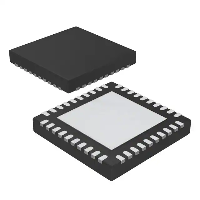
- Part No.:
- PN7160A1HN/C100Y
- Manufacturer:
- NXP Semiconductors
- Category:
- RFID, RF Access, Monitoring ICs
- Package:
- 40-VFQFN Exposed Pad
- Datasheet:
-
 PN7160A1HN/C100Y.pdf
- Description:
- IC NFC CONTROLLER I2C HVQFN40
- Quantity:
- Payment:

- Shipping:

Inventory:1,092
Please send an inquiry. Send us your inquiry, and we will respond immediately.
Product details
Overview
PN7160A1HN/C100Y from NXP Semiconductors is a Near Field Communication (NFC) controller IC with integrated NCI 2.0 interface and firmware, designed for mobile and portable devices requiring ISO/IEC 14443A/B, ISO/IEC 15693, MIFARE, and FeliCa support. It delivers 1.3 W transmitter output power, 20 mV(p-p) card-mode receiver sensitivity, and operates across 2.8–5.5 V battery supply. Used in smartphone NFC subsystems for secure contactless transactions and card emulation.
For engineers reviewing the PN7160A1HN/C100Y datasheet, PN7160A1HN/C100Y pinout, PN7160A1HN/C100Y application, or PN7160A1HN/C100Y equivalent, this page provides verified technical context, HVQFN40 package mapping, autonomous low-power polling loop behavior, and confirmed alternative options for NFC controller selection in mobile and embedded designs.
Technical Context
The PN7160A1HN/C100Y implements an NCI 2.0–compliant host interface over I²C (High-Speed mode), supports firmware-controlled autonomous operation in Standby and Hard Power Down states, and integrates a dual-output RF front-end (TX1/TX2) with dynamic power control and Enhanced Dynamic Load Modulation Amplitude (DLMA). Its ARM Cortex-M0 core executes embedded firmware for tag emulation, reader/writer, and P2P passive modes up to 424 kbps.
It features a dedicated 27.12 MHz crystal oscillator input (NFC_CLK_XTAL1), integrated PLL, buffered antenna drivers, and independent LMA phase adjustment (5° steps for Type A/B/F). The device supports external DC-DC enable (DCDC_EN) and wake-up via RF field, internal timer, or host request (WKUP_REQ), enabling true "host-off" card emulation without system-level power.
Key Specifications
| Parameter | Value and Actual Design Meaning |
|---|---|
| Battery Supply Range | 2.8 V to 5.5 V - enables direct connection to Li-ion/Li-poly battery rails without external regulators. |
| Transmitter Output Power | 1.3 W - supports extended read range and robust communication with small-form-factor antennas. |
| Card Mode Sensitivity | 20 mV(p-p) - ensures reliable detection of weak-field cards and tags in noisy environments. |
| Host Interface | I²C High-Speed mode - reduces host-side latency and simplifies integration with application processors. |
| Firmware Version | 12.50.05 - production firmware supporting T4T NDEF write from RF side and full ISO/IEC 14443A/B PICC/PCD modes. |
| Power Consumption (Standby) | 32–52 μA - ultra-low quiescent current enables multi-day background polling in wearable devices. |
| Ambient Operating Temperature | −30 °C to +85 °C - qualified for consumer and industrial portable equipment deployment. |
Pinout & Package
HVQFN40 (SOT618-1) package: 40-terminal, thermally enhanced, leadless quad flat package with exposed thermal pad (VSS center pad). Dimensions: 6.0 mm × 6.0 mm × 0.85 mm (max height).
| Pin/Terminal | Circuit Role | Design Meaning |
|---|---|---|
| 1 (I2C_ADR0/SPI_NSS) | Host interface select / chip enable | Configures I²C address or SPI slave select; sets interface mode at boot. |
| 8 (IRQ) | Interrupt request output | Active-low signal alerts host of RF events, command completions, or wake-up triggers. |
| 10 (VEN) | Hard Power Down control | Low-voltage assertion (<0.4 V) forces HPD state; high voltage enables normal operation. |
| 15/16 (RXN/RXP) | Differential receiver inputs | Accepts analog RF signals from antenna matching network; enables single-ended receiver option. |
| 19/21 (TX2/TX1) | RF transmitter outputs | Drive antenna coil in push-pull configuration; support up to 250 mA continuous current per path. |
| 23/24 (ANT1/ANT2) | Antenna wake-up sense inputs | Enable RF-field-triggered wake-up while in Standby, independent of host power state. |
| 37 (DCDC_EN) | External DC-DC enable request | Signals external regulator (e.g., PCA941xA) to boost TX supply voltage for higher output power. |
| 39 (WKUP_REQ) | Wake-up request input | Allows host to initiate transition from Standby to Active state on demand. |
Key Features
| Feature | Design Value |
|---|---|
| Autonomous Card Emulation | Operates in Standby with host powered off; presents NDEF data via T4T emulation without CPU intervention. |
| Dynamic Power Control (DPC) | Adjusts transmitter output in real time to maximize range while staying within ISO 14443 field strength limits. |
| Enhanced DLMA | Adaptively optimizes load modulation amplitude based on external RF field strength, extending card-mode range. |
| Integrated Polling Loop | Hardware-accelerated discovery sequence reduces host CPU load and enables sub-500 ms polling intervals. |
| Anti-Tearing Support | Non-volatile EEPROM (28 kB) includes hardware recovery logic to prevent corruption during unexpected power loss. |
| Flexible Clock Architecture | Supports 27.12 MHz crystal (NFC_CLK_XTAL1/XTAL2) or external clock; integrated PLL eases timing margining. |
Applications
| Smartphone Secure Element Interface | Wearable Contactless Payment |
|---|---|
|
Use Scenario: Integration between application processor and secure element (e.g., eSE or UICC) in Android smartphones for HCE and SE-based transactions. IC Role / Device Role / Timing Role: NFC controller handling NCI 2.0 protocol translation, RF framing, and secure channel management between host and SE. Use Value: Enables certified EMVCo Level 1 compliance with <200 ms transaction latency and autonomous wake-up from deep sleep on tap. |
Use Scenario: Enabling tap-to-pay functionality in fitness trackers and smartwatches with constrained battery capacity. IC Role / Device Role / Timing Role: Standalone NFC interface executing card emulation autonomously while main MCU remains in low-power retention mode. Use Value: Achieves >7-day background polling life using only 32–52 μA standby current and RF-triggered wake-up. |
| Tablet Access Control Reader | Smart Home Gateway Tag Provisioning |
|
Use Scenario: Embedded NFC reader in enterprise tablets used for physical access badge verification and credential enrollment. IC Role / Device Role / Timing Role: Reader/writer controller supporting ISO/IEC 14443A/B, MIFARE DESFire, and FeliCa protocols with fast tag polling. Use Value: Delivers 1.3 W output power and 20 mV(p-p) sensitivity to reliably read badges at 50+ mm distance with compact PCB antennas. |
Use Scenario: NFC-enabled home gateway provisioning IoT devices (e.g., smart locks, sensors) via NDEF-configured setup tokens. IC Role / Device Role / Timing Role: Host-managed initiator that writes encrypted configuration records to unpowered NFC tags during onboarding. Use Value: Leverages integrated EEPROM and anti-tearing to ensure atomic NDEF write operations even during brown-out conditions. |
Equivalent & Alternatives
The following parts are listed as comparable options for similar NFC controller applications.
| Alternative Part | Technical Difference | Application Difference | Selection Advice |
|---|---|---|---|
| PN7160A1EV/C100Y | VFBGA64 package (64-ball); identical firmware (12.50.05) and I²C interface; smaller footprint but requires microvia routing. | Better suited for space-constrained mobile designs where board area is prioritized over thermal dissipation. | Select when PCB stack-up supports fine-pitch BGA and thermal management is handled via internal layers. |
| PN7161A1HN/C100Y | HVQFN40 package; adds Apple Enhanced Contactless Polling (ECP) support (requires formal authorization); same firmware version. | Required for iOS accessory certification and ECP-compliant reader implementations targeting Apple ecosystem interoperability. | Choose only if ECP functionality is contractually mandated and authorization has been obtained from Apple. |
Compared with PN7160A1HN/C100Y, the VFBGA64 variant offers denser integration but less thermal headroom, while the PN7161A1HN/C100Y adds ECP capability at no pinout or power cost-making it a drop-in upgrade only when ECP is required and authorized.
Availability
PN7160A1HN/C100Y is available at Aetrix Electronics and suitable for smartphone NFC subsystems, wearable payment terminals, tablet access readers, and smart home gateways requiring stable component supply, long-term lifecycle support, and RoHS-compliant manufacturing.
Supply support for PN7160A1HN/C100Y includes scheduled delivery planning, volume procurement assistance, BOM continuity management, traceable sourcing, and lifecycle availability coordination for OEM customers, industrial embedded developers, connected-device designers, and electronics production programs.
Manufacturer
NXP Semiconductors is a global semiconductor leader specializing in secure connectivity solutions for automotive, industrial, and mobile markets, with over 20 years of NFC innovation and industry-standardization leadership.
PN7160A1HN/C100Y belongs to NXP's PN716x NFC controller family, engineered to simplify NFC integration in battery-powered devices by minimizing external components, enabling host-off operation, and delivering certified interoperability with global contactless infrastructure.
FAQ
What is the primary interface protocol supported by PN7160A1HN/C100Y?
PN7160A1HN/C100Y implements the NFC Forum NCI 2.0 standard as its primary logical host interface, with physical layer support for I²C High-Speed mode (up to 3.4 Mbps). This enables seamless integration with Android and Linux-based application processors while maintaining strict compliance with NFC Forum digital protocol requirements. The PN7160A1HN/C100Y does not support UART or USB natively.
Does PN7160A1HN/C100Y support card emulation without host processor involvement?
Yes, PN7160A1HN/C100Y supports autonomous card emulation in Standby mode. When configured by the host and placed in Autonomous mode, it can present T4T-compliant NDEF data via ISO/IEC 14443A emulation-even with the host processor fully powered down. This capability relies on its integrated 28 kB EEPROM and dedicated RF front-end, making PN7160A1HN/C100Y ideal for always-on contactless use cases.
What is the maximum continuous transmitter current supported by PN7160A1HN/C100Y?
PN7160A1HN/C100Y supports up to 250 mA continuous current per transmitter path (TX1/TX2) when operating in PCD mode, as specified in Table 1 of the datasheet. This limit ensures compliance with ISO/IEC 14443 field strength requirements and prevents antenna overheating. The device includes a programmable current limiter (Ith(Ilim) = 270–330 mA) to enforce this boundary in real time.
Can PN7160A1HN/C100Y operate with a 3.3 V-only supply?
PN7160A1HN/C100Y requires separate supplies: VBAT (2.8–5.5 V) for RF and core functions, and VDD(PAD) (3.0–3.6 V) for the I²C interface. A 3.3 V rail alone cannot power both domains. Using 3.3 V for VDD(PAD) is valid, but VBAT must be ≥2.8 V-typically supplied from a battery or buck converter. The PN7160A1HN/C100Y does not support single-rail 3.3 V operation.
Is PN7160A1HN/C100Y compatible with Apple's Enhanced Contactless Polling (ECP)?
No, PN7160A1HN/C100Y does not support Apple ECP. That feature is exclusive to the PN7161 family (e.g., PN7161A1HN/C100Y), which shares the same HVQFN40 package and pinout but requires formal Apple authorization for ECP activation. PN7160A1HN/C100Y implements all baseline NFC Forum and EMVCo protocols-including T4T, ISO/IEC 14443A/B, and MIFARE-but excludes ECP-specific firmware and certification paths.
PN7160A1HN/C100Y Specifications
- Product attributes
- Attribute value
- Manufacturer:
- NXP Semiconductors
- Series:
- -
- Package/Case:
- 40-VFQFN Exposed Pad
- Packaging:
- Tape & Reel (TR)
- Product Status:
- Active
- Type:
- RFID Reader
- Frequency:
- 13.56MHz
- Standards:
- FeliCa, ISO 14443, ISO 15693, MIFARE, NFC
- Interface:
- I2C
- Voltage - Supply:
- 1.65V ~ 1.95V, 3V ~ 3.6V
- Operating Temperature:
- -25°C ~ 85°C (TA)
- Grade:
- -
- Qualification:
- -
- Mounting Type:
- Surface Mount
- Supplier Device Package:
- 40-HVQFN (6x6)
PN7160A1HN/C100Y FAQ
1.How can I place an order for PN7160A1HN/C100Y through Aetrix?
Please submit a Request for Quotation (RFQ) for PN7160A1HN/C100Y on Aetrix. Our sales agent will provide a competitive quotation and guide you through the order confirmation once you accept the terms.
2.Are the price and stock information for PN7160A1HN/C100Y reliable?
The price and inventory of PN7160A1HN/C100Y are updated periodically and may fluctuate due to market conditions. Stock and pricing data are typically refreshed every 24 hours. Quotation validity for PN7160A1HN/C100Y is usually 5 days.
3.What payment methods are accepted for PN7160A1HN/C100Y?
We accept Wire Transfer, PayPal, Credit Card, Western Union, MoneyGram, and Escrow for PN7160A1HN/C100Y transactions.
Note: Certain payment methods may incur a processing fee.
4.How is shipping managed for PN7160A1HN/C100Y?
PN7160A1HN/C100Y orders can be shipped via leading logistics carriers, including DHL, UPS, FedEx, TNT, or Registered Mail.
Once your PN7160A1HN/C100Y order is processed, you will receive an email with the shipment details and tracking number.
Note: Tracking information may take up to 24 hours to appear. Express delivery typically takes 3–5 business days.
5.How can I obtain technical support or documentation for PN7160A1HN/C100Y?
For technical support, including PN7160A1HN/C100Y datasheets, pinout diagrams, or application guidance, please contact our engineering support team. They can provide detailed documentation and assistance for your PN7160A1HN/C100Y requirements.
6.How does Aetrix verify that PN7160A1HN/C100Y is sourced from the original manufacturer or authorized distributors?
All PN7160A1HN/C100Y products on Aetrix are procured from qualified distributors and authorized channels. Our dedicated quality assurance team conducts strict verification, including traceability checks and, if necessary, third-party testing. This ensures that PN7160A1HN/C100Y meets industry standards.
7.What is the process for return or replacement of PN7160A1HN/C100Y?
All PN7160A1HN/C100Y units undergo pre-shipment inspection (PSI). If there is an issue with PN7160A1HN/C100Y, returns or replacements are accepted under the following conditions:
1.Quantity discrepancies, incorrect items, or visible external defects (such as breakage or corrosion), acknowledged by Aetrix.
2.The issue is reported within 90 days of delivery.
3.The PN7160A1HN/C100Y part is unused and in its original packaging.
Return procedure for PN7160A1HN/C100Y:
1.Submit a request within 90 days.
2.Obtain a Return Material Authorization (RMA) from Aetrix.
PN7160A1HN/C100Y Tags

-
SL2S2602FTBX
NXP Semiconductors

-
ST25DV04K-IER6S3
STMicroelectronics

-
ST25DV04K-IER6C3
STMicroelectronics
-
LXMSJZNCMD-217
Murata Electronics

-
NT3H2111W0FTTJ
NXP Semiconductors

-
NT3H2111W0FHKH
NXP Semiconductors

-
M24LR04E-RMC6T/2
STMicroelectronics
-
ST25DV04KC-JF6D3
STMicroelectronics

-
ST25DV64KC-IE6S3
STMicroelectronics

-
ST25DV64K-IER6T3
STMicroelectronics
-
NT3H2211W0FTTJ
NXP Semiconductors
-
NT3H2211W0FHKH
NXP Semiconductors
Tech Hub

A practical engineering guide to 3.3V and 5V logic compatibility, input thresholds, resistor dividers, translator ICs, MOSFET level shifting, I2C pull-ups, timing limits and power-sequencing risks.

The 74HC595 uses push-pull logic outputs, while the TPIC6B595 uses 50 V open-drain DMOS sinks for higher-power loads. This guide compares timing, current limits, 3.3 V interfacing, load wiring, thermal…

The 74HC595 converts serial data into eight stable parallel outputs. This guide covers pin functions, shift and storage timing, OE and MR behavior, drive-current limits, cascading, voltage compatibilit…

A technical comparison of level-sensitive latches and edge-triggered flip-flops, covering timing windows, setup and hold limits, master–slave operation, time borrowing, race-through, HDL inference and…

A D latch stores one bit while Enable controls when data can pass. This reference covers gate-level operation, truth tables, transparency, setup and hold timing, LE versus OE, common ICs and practical …

An SR latch stores one bit through cross-coupled feedback. This engineering reference covers NOR and NAND implementations, truth tables, forbidden-state recovery, gated operation, switch debouncing, fa…

Latch circuits retain one bit through feedback. This technical reference covers SR and D latches, truth tables, transparency, timing limits, latch-versus-flip-flop behavior, applications and common log…

An engineering guide to LED driver operation, constant-current and constant-voltage outputs, linear and switching topologies, dimming, IC selection, calculations, replacement compatibility, and fault c…

Operational amplifier guide covering op amp basics, feedback, ideal vs real op amps, common configurations, buffer circuits, offset, bias current, gain-bandwidth, slew rate, rail-to-rail limits and sel…

Jumper cables guide covering safe connection order, red and black clamp placement, final ground connection, cable gauge, length, clamp quality, copper vs CCA cables, jump starter comparison and battery…


