Send an Inquiry

To receive a quote for your project, please fill in the following information, and we’ll get back to you promptly.

Name*
Company*
Email Address*
Phone/WhatsApp
Part Number*
Quantity*
Message
Submit Inventory List

Please fill in the following information, and we’ll get back to you promptly.

Name*
Company*
Email Address*
Phone/WhatsApp
Upload My List
Message

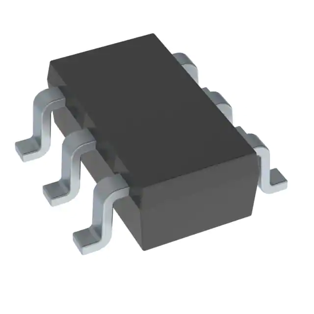
Vishay Siliconix SI3495DV-T1-GE3

Part No.:
SI3495DV-T1-GE3
Manufacturer:
Vishay Siliconix
Category:
FETs, MOSFETs
Package:
SOT-23-6 Thin, TSOT-23-6
Datasheet:
AetrixSI3495DV-T1-GE3.pdf
Description:
MOSFET P-CH 20V 5.3A 6TSOP
Quantity:
Payment:
Payment
Shipping:
Shipping

Inventory:9,445

Please send an inquiry. Send us your inquiry, and we will respond immediately.

Part Number
Quantity*
Price
Name*
Company
Email*
Comments

Product details

Overview

SI3495DV-T1-GE3 from Vishay Siliconix is a P-channel TrenchFET® power MOSFET rated for -20 V drain-source voltage, -7 A continuous drain current at 25 °C, and ultra-low on-resistance of 0.024 Ω at VGS = -4.5 V. It serves as a load or PA switch in portable electronics with 1.5 V gate threshold compatibility and halogen-free, RoHS-compliant construction.

For engineers reviewing the SI3495DV-T1-GE3 datasheet, SI3495DV-T1-GE3 pinout, SI3495DV-T1-GE3 application, or SI3495DV-T1-GE3 equivalent, key selection criteria include its -1.5 V gate-rated operation, TSOP-6 package thermal performance (RthJA = 62.5 °C/W max), integrated body diode characteristics, and verified Rg testing for switching consistency in battery-powered switching circuits.

Technical Context

This device operates as a logic-level P-channel enhancement-mode MOSFET with a guaranteed gate threshold voltage range of -0.35 V to -0.75 V, enabling reliable turn-on from low-voltage controllers. Its trench-based silicon structure delivers stable RDS(on) across temperature and gate drive conditions, supporting robust load switching down to VGS = -1.5 V.

The TSOP-6 package provides optimized thermal path to PCB via exposed drain pad, with RthJF ≤ 30 °C/W steady-state, and supports pulsed drain currents up to -20 A. Dynamic parameters-including Qg = 38 nC max, td(off) = 300 ns max, and VSD = -1.1 V max-confirm suitability for high-efficiency, fast-switching DC load control.

Key Specifications

ParameterValue and Actual Design Meaning
VDS-20 V - Maximum blocking voltage for battery-side high-side switching in 3.3 V/5 V systems
RDS(on)0.024 Ω @ VGS = -4.5 V - Enables <170 mW conduction loss at 7 A, critical for thermal management in compact layouts
ID (continuous)-7 A @ TA = 25 °C - Supports sustained load switching in handheld power rails without forced cooling
VGS(th)-0.75 V max - Ensures full enhancement with 1.8 V GPIO or low-voltage PMIC outputs
Qg38 nC max - Determines gate drive energy requirement for <50 ns rise/fall in 1 MHz-class switching
RthJA62.5 °C/W max - Defines junction-to-ambient thermal limit on standard FR4, guiding heatsinking decisions
VSD-1.1 V max @ IS = -1.7 A - Quantifies forward drop of integrated body diode during reverse-current recovery

Pinout & Package

TSOP-6 surface-mount package with exposed drain pad for thermal dissipation; 2.85 mm × 3.0 mm footprint, 1.0 mm max height.

Pin/TerminalCircuit RoleDesign Meaning
1, 2, 5, 6Drain (D)Common high-current output node; internally connected to exposed pad for low-inductance, low-thermal-resistance path
3Gate (G)Control input requiring <38 nC charge for full enhancement; sensitive to ESD (±5 V rating)
4Source (S)Reference node for gate drive; connects to system ground or battery return in high-side configuration

Key Features

FeatureDesign Value
TrenchFET® architectureDelivers 0.024 Ω RDS(on) at -4.5 V while maintaining -20 V VDS rating-enabling compact, efficient load switches
100 % Rg testedGuarantees gate resistance between 4 Ω and 13 Ω, ensuring predictable turn-on timing and drive circuit stability
Halogen-free & RoHS-compliantMeets IEC 61249-2-21 and Directive 2002/95/EC-required for consumer electronics export compliance
Logic-level gate driveOperates fully enhanced down to VGS = -1.5 V, eliminating need for level-shifting in 1.8 V/2.5 V controller interfaces

Applications

Battery-Powered Load SwitchingRF Power Amplifier Enable Control

Use Scenario: Managing power delivery to subsystems (e.g., display backlight, USB peripheral) in smartphones and wearables during sleep/wake cycles.

IC Role / Device Role / Timing Role: High-side P-channel switch controlled by baseband processor GPIO; placed between battery and load rail.

Use Value: Low RDS(on) minimizes voltage droop and self-heating; -1.5 V VGS(th) ensures clean turn-on with 1.8 V logic signals.

Use Scenario: Enabling/disabling RF power amplifier stages in LTE/5G front-end modules to reduce standby current.

IC Role / Device Role / Timing Role: Fast-turning enable switch placed between bias supply and PA collector/drain rail.

Use Value: 300 ns max td(off) and 160 ns max fall time support rapid PA shutdown, meeting 3GPP transient response requirements.

USB OTG Power Path ManagementPortable Medical Sensor Power Gating

Use Scenario: Isolating VBUS from downstream devices during host/peripheral role negotiation in USB On-The-Go implementations.

IC Role / Device Role / Timing Role: Bidirectional load switch controlling current flow direction between USB port and device battery or regulator.

Use Value: Integrated body diode with -1.1 V VSD enables reverse-current protection without external components; TSOP-6 footprint saves board space.

Use Scenario: Power gating discrete sensor ICs (e.g., ECG, SpO₂) in handheld diagnostic tools to extend battery life between measurements.

IC Role / Device Role / Timing Role: Low-leakage (IDSS ≤ -1 µA) high-side switch isolating sensor supply rail during idle periods.

Use Value: -10 µA IDSS at 85 °C ensures <1 µA total system leakage, preserving multi-week shelf life in battery-critical medical applications.

Equivalent & Alternatives

The following parts are listed as comparable options for similar P-channel load switch applications.

Alternative PartTechnical DifferenceApplication DifferenceSelection Advice
Si3485DV-T1-GE3Same TSOP-6 package, -20 V rating, but higher RDS(on) (0.032 Ω @ -4.5 V) and lower ID (-5.3 A)Lower current capability limits use in >5 A loads; suitable where thermal margin allows higher on-lossSelect when cost sensitivity outweighs conduction loss requirements and peak load current stays below 5 A
DMN2011LFG-720 V P-channel, 0.022 Ω @ -4.5 V, but SOT-23-6 package with higher RthJA (125 °C/W)Reduced thermal performance restricts continuous current to ~3.5 A on standard PCB; smaller footprintChoose for space-constrained designs accepting derated current or intermittent duty cycling

Compared with Si3485DV-T1-GE3 and DMN2011LFG-7, the SI3495DV-T1-GE3 offers superior thermal handling (62.5 °C/W vs. ≥125 °C/W) and higher continuous current (7 A vs. ≤5.3 A), making it optimal for sustained-load portable power switching where board area permits TSOP-6 placement.

Availability

SI3495DV-T1-GE3 is available at Aetrix Electronics and suitable for battery-powered load switching, RF power amplifier enable control, and USB OTG power path management requiring stable component supply, halogen-free compliance, and verified gate-drive compatibility with low-voltage microcontrollers.

Supply support for SI3495DV-T1-GE3 includes scheduled delivery planning, volume procurement assistance, BOM continuity management, traceable sourcing, and lifecycle availability coordination for OEM customers, industrial embedded developers, connected-device designers, and electronics production programs.

Manufacturer

Vishay Siliconix is a global leader in discrete semiconductors, specializing in MOSFETs, diodes, and optoelectronics with emphasis on power efficiency, reliability, and miniaturization.

The Si3495DV-T1-GE3 belongs to Vishay's TrenchFET® logic-level P-channel MOSFET product line, engineered specifically for high-efficiency, low-voltage load switching in space- and thermally-constrained portable electronics.

FAQ

What is the maximum continuous drain current rating for SI3495DV-T1-GE3 at 85 °C ambient?

The SI3495DV-T1-GE3 supports -3.6 A continuous drain current at TA = 85 °C with no heatsink on a 1" × 1" FR4 board. This derating reflects its RthJA = 62.5 °C/W maximum and 150 °C maximum junction temperature. Designers must verify layout thermal performance using the normalized transient impedance curves in the datasheet to confirm safe operation under actual PCB conditions. The SI3495DV-T1-GE3 datasheet specifies this value explicitly in the Absolute Maximum Ratings table.

Does SI3495DV-T1-GE3 have a specified gate charge value for design of driver circuits?

Yes, the SI3495DV-T1-GE3 has a total gate charge (Qg) of 38 nC maximum at VDS = -10 V, VGS = -4.5 V, and ID = -7 A. This parameter directly determines the required gate driver current and energy per switching cycle. The SI3495DV-T1-GE3 also specifies Qgs = 2.5 nC and Qgd = 7 nC, enabling accurate calculation of Miller plateau timing. These values are measured and guaranteed per the datasheet revision C test conditions.

Is SI3495DV-T1-GE3 suitable for reverse-polarity protection in 5 V systems?

Yes, the SI3495DV-T1-GE3 is appropriate for reverse-polarity protection in 5 V systems due to its -20 V VDS rating, low RDS(on) (0.024 Ω), and integrated body diode with VSD ≤ -1.1 V. When placed in the high-side position with source tied to input and drain to load, it blocks reverse current while conducting forward current with minimal drop. The SI3495DV-T1-GE3's -1.5 V gate threshold ensures reliable turn-on from standard 5 V regulators or LDOs without additional level shifting.

What is the gate-to-source leakage specification for SI3495DV-T1-GE3?

The SI3495DV-T1-GE3 specifies gate-to-source leakage (IGSS) as ±100 nA maximum at VDS = 0 V and VGS = ±5 V. This low leakage supports stable gate bias in high-impedance drive circuits and ensures minimal power loss in always-on control nodes. The value is measured per the datasheet's Electrical Characteristics table and applies across the full operating temperature range of -55 °C to +150 °C. All SI3495DV-T1-GE3 units undergo screening to meet this specification.

How does the thermal performance of SI3495DV-T1-GE3 compare between junction-to-ambient and junction-to-foot?

The SI3495DV-T1-GE3 has a maximum steady-state junction-to-ambient thermal resistance (RthJA) of 110 °C/W and a much lower junction-to-foot (drain pad) resistance (RthJF) of 30 °C/W. This 3.7× improvement confirms that thermal performance is highly dependent on PCB copper area connected to the exposed drain pad. For optimal results, the SI3495DV-T1-GE3 datasheet recommends ≥1 cm² of 2-oz copper under the pad, which can reduce effective RthJA to near the 62.5 °C/W typical value cited in the Absolute Maximum Ratings.

SI3495DV-T1-GE3 Specifications

Product attributes
Attribute value
Manufacturer:
Vishay Siliconix
Series:
TrenchFET®
Package/Case:
SOT-23-6 Thin, TSOT-23-6
Packaging:
Tape & Reel (TR)
Product Status:
Obsolete
FET Type:
P-Channel
Technology:
MOSFET (Metal Oxide)
Drain to Source Voltage (Vdss):
20 V
Current - Continuous Drain (Id) @ 25°C:
5.3A (Ta)
Drive Voltage (Max Rds On, Min Rds On):
1.5V, 4.5V
Rds On (Max) @ Id, Vgs:
24mOhm @ 7A, 4.5V
Vgs(th) (Max) @ Id:
750mV @ 250µA
Gate Charge (Qg) (Max) @ Vgs:
38 nC @ 4.5 V
Vgs (Max):
±5V
Input Capacitance (Ciss) (Max) @ Vds:
-
FET Feature:
-
Power Dissipation (Max):
1.1W (Ta)
Operating Temperature:
-55°C ~ 150°C (TJ)
Grade:
-
Qualification:
-
Mounting Type:
Surface Mount
Supplier Device Package:
6-TSOP

SI3495DV-T1-GE3 FAQ

1.How can I place an order for SI3495DV-T1-GE3 through Aetrix?

Please submit a Request for Quotation (RFQ) for SI3495DV-T1-GE3 on Aetrix. Our sales agent will provide a competitive quotation and guide you through the order confirmation once you accept the terms.

2.Are the price and stock information for SI3495DV-T1-GE3 reliable?

The price and inventory of SI3495DV-T1-GE3 are updated periodically and may fluctuate due to market conditions. Stock and pricing data are typically refreshed every 24 hours. Quotation validity for SI3495DV-T1-GE3 is usually 5 days.

3.What payment methods are accepted for SI3495DV-T1-GE3?

We accept Wire Transfer, PayPal, Credit Card, Western Union, MoneyGram, and Escrow for SI3495DV-T1-GE3 transactions.

Note: Certain payment methods may incur a processing fee.

4.How is shipping managed for SI3495DV-T1-GE3?

SI3495DV-T1-GE3 orders can be shipped via leading logistics carriers, including DHL, UPS, FedEx, TNT, or Registered Mail.

Once your SI3495DV-T1-GE3 order is processed, you will receive an email with the shipment details and tracking number.

Note: Tracking information may take up to 24 hours to appear. Express delivery typically takes 3–5 business days.

5.How can I obtain technical support or documentation for SI3495DV-T1-GE3?

For technical support, including SI3495DV-T1-GE3 datasheets, pinout diagrams, or application guidance, please contact our engineering support team. They can provide detailed documentation and assistance for your SI3495DV-T1-GE3 requirements.

6.How does Aetrix verify that SI3495DV-T1-GE3 is sourced from the original manufacturer or authorized distributors?

All SI3495DV-T1-GE3 products on Aetrix are procured from qualified distributors and authorized channels. Our dedicated quality assurance team conducts strict verification, including traceability checks and, if necessary, third-party testing. This ensures that SI3495DV-T1-GE3 meets industry standards.

7.What is the process for return or replacement of SI3495DV-T1-GE3?

All SI3495DV-T1-GE3 units undergo pre-shipment inspection (PSI). If there is an issue with SI3495DV-T1-GE3, returns or replacements are accepted under the following conditions:

1.Quantity discrepancies, incorrect items, or visible external defects (such as breakage or corrosion), acknowledged by Aetrix.

2.The issue is reported within 90 days of delivery.

3.The SI3495DV-T1-GE3 part is unused and in its original packaging.

Return procedure for SI3495DV-T1-GE3:

1.Submit a request within 90 days.

2.Obtain a Return Material Authorization (RMA) from Aetrix.

SI3495DV-T1-GE3 Tags
  • SI3495DV-T1-GE3
  • SI3495DV-T1-GE3 PDF
  • SI3495DV-T1-GE3 Datasheet
  • SI3495DV-T1-GE3 Specifications
  • SI3495DV-T1-GE3 Images
  • Vishay Siliconix
  • Vishay Siliconix SI3495DV-T1-GE3
  • Buy SI3495DV-T1-GE3
  • SI3495DV-T1-GE3 Price
  • SI3495DV-T1-GE3 Distributor
  • SI3495DV-T1-GE3 Supplier
  • SI3495DV-T1-GE3 Wholesale
Related Products
BSZ180P03NS3EGATMA1
BSZ180P03NS3EGATMA1

Infineon Technologies
SIRA14DP-T1-GE3
SIRA14DP-T1-GE3

Vishay Siliconix

AO4419
AO4419

Alpha & Omega Semiconductor Inc.
SISA14BDN-T1-GE3
SISA14BDN-T1-GE3

Vishay Siliconix

PSMN9R5-30YLC,115
PSMN9R5-30YLC,115

Nexperia USA Inc.

BUK9Y21-40E,115
BUK9Y21-40E,115

Nexperia USA Inc.

RTQ035N03HZGTR
RTQ035N03HZGTR

Rohm Semiconductor

FDMS7680
FDMS7680

onsemi

RQ3E180BNTB
RQ3E180BNTB

Rohm Semiconductor

STL6N2VH5
STL6N2VH5

STMicroelectronics

DMPH4029LFGQ-7
DMPH4029LFGQ-7

Diodes Incorporated

DMT6015LSS-13
DMT6015LSS-13

Diodes Incorporated

Tech Hub

Search

Search

PRODUCT

PRODUCT

PHONE

PHONE

USER

USER