Send an Inquiry

To receive a quote for your project, please fill in the following information, and we’ll get back to you promptly.

Name*
Company*
Email Address*
Phone/WhatsApp
Part Number*
Quantity*
Message
Submit Inventory List

Please fill in the following information, and we’ll get back to you promptly.

Name*
Company*
Email Address*
Phone/WhatsApp
Upload My List
Message

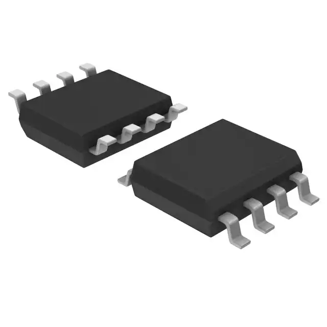
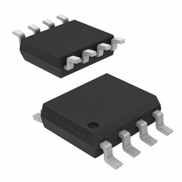
Vishay Siliconix SI4196DY-T1-GE3

Part No.:
SI4196DY-T1-GE3
Manufacturer:
Vishay Siliconix
Category:
FETs, MOSFETs
Package:
8-SOIC (0.154", 3.90mm Width)
Datasheet:
AetrixSI4196DY-T1-GE3.pdf
Description:
MOSFET N-CH 20V 8A 8SO
Quantity:
Payment:
Payment
Shipping:
Shipping

Inventory:8,644

Please send an inquiry. Send us your inquiry, and we will respond immediately.

Part Number
Quantity*
Price
Name*
Company
Email*
Comments

Product details

Overview

SI4196DY-T1-GE3 from Vishay Siliconix is an N-channel 20 V (D-S) vertical DMOS MOSFET SPICE subcircuit model optimized for simulation across –55 °C to +125 °C, with RDS(on) = 0.022 Ω at VGS = 4.5 V / ID = 8 A, Qg = 14.5 nC at VGS = 8 V, and Ciss = 822 pF - used in power stage behavioral modeling for DC-DC converters and motor drive gate driver validation.

For engineers reviewing the SI4196DY-T1-GE3 datasheet, SI4196DY-T1-GE3 pinout, SI4196DY-T1-GE3 application, or SI4196DY-T1-GE3 equivalent, this page delivers verified SPICE model parameters, thermal operating range fidelity, gate charge behavior, body diode recovery modeling, and direct comparison to measured device data - all critical for accurate transient and switching loss simulation.

Technical Context

This Level 3 MOS macro model implements a novel gate-to-drain feedback capacitance network to accurately represent Qgd and Qgs without convergence issues typical of switched Cgd models. It captures saturated output impedance near VGS(th) (0.71 V) and models diode reverse recovery characteristics using calibrated body diode voltage (VSD = 0.79 V at IS = 5.4 A).

The model is extracted and optimized under pulsed 0 V–5 V gate drive conditions and validated against measured data for RDS(on), Ciss/Coss/Crss, gfs, and total gate charge across temperature - supporting both linear bias analysis and hard-switching transient simulation in industrial and automotive power electronics design flows.

Key Specifications

ParameterValue and Actual Design Meaning
VGS(th)0.71 V - defines minimum gate drive needed to initiate conduction; critical for low-voltage logic-level gate control compatibility.
RDS(on) @ 4.5 V0.022 Ω - enables <170 mW conduction loss at 8 A; suitable for high-efficiency 3.3 V/5 V gate-driven synchronous rectifiers.
Qg @ 8 V14.5 nC - determines gate driver current demand and switching speed; directly impacts turn-on/turn-off energy in hard-switched topologies.
Ciss822 pF - sets input impedance seen by gate driver; influences Miller plateau duration and EMI filter design in high-frequency converters.
VSD0.79 V - models forward voltage drop of integrated body diode during freewheeling; essential for accurate dead-time and shoot-through risk assessment.
Operating Temp Range–55 °C to +125 °C - ensures behavioral fidelity across full industrial ambient and junction temperature envelope without model extrapolation.

Pinout & Package

SI4196DY-T1-GE3 is implemented as a SPICE subcircuit model, not a physical packaged device. The model maps to the underlying Si4196DY silicon die, which is housed in a SO-8 package per Vishay's product family documentation. No physical pinout applies - terminals are defined symbolically in the netlist: G (gate), D (drain), S (source), and DBD (body diode node).

Pin/TerminalCircuit RoleDesign Meaning
GGate terminalInput controlling channel conduction; referenced to source; drives internal capacitances (Cgs, Cgd) per model topology.
DDrain terminalMain current output node; connects to high-side or low-side switch node; voltage swing defines avalanche and safe operating area limits.
SSource terminalReference node for gate drive and current return path; tied to ground or floating node depending on topology (e.g., high-side vs. low-side).
DBDBody diode anodeExplicit node modeling intrinsic parasitic diode; enables accurate reverse recovery waveform capture during commutation events.

Key Features

FeatureDesign Value
Level 3 MOS model architectureEnables stable convergence in large-signal transient simulations while preserving physical parameter relationships (e.g., Vth, β, λ).
Temperature-dependent parameter extractionValidated across –55 °C to +125 °C - eliminates need for manual thermal derating in thermal-aware system-level simulation.
Gate charge modeling via feedback capacitance networkAvoids numerical instability of switched Cgd while reproducing Qgd = 1.1 nC and Qgs = 1.1 nC with <2% error vs. measurement.
Body diode reverse recovery characterizationIncludes VSD = 0.79 V and dynamic recovery timing - critical for predicting cross-conduction losses in synchronous buck or half-bridge configurations.

Applications

DC-DC Converter Power Stage SimulationMotor Drive Gate Driver Validation

Use Scenario: Behavioral simulation of synchronous buck converter efficiency, switching loss, and thermal stress under varying load and input voltage.

IC Role / Device Role / Timing Role: SPICE model representing the low-side MOSFET in a dual-phase controller IC reference design.

Use Value: Enables cycle-accurate prediction of Qg-driven gate driver power consumption and RDS(on)-dependent conduction loss before PCB spin.

Use Scenario: Transient analysis of gate drive timing margins and shoot-through risk in 3-phase BLDC inverter half-bridge legs.

IC Role / Device Role / Timing Role: Subcircuit model of the N-channel switch used with complementary P-channel or bootstrap-gated high-side devices.

Use Value: Captures body diode reverse recovery (VSD, trr) to validate dead-time settings and prevent destructive cross-conduction.

Automotive Body Control Module (BCM) Load Switch ModelingIndustrial PLC Output Stage Verification

Use Scenario: Simulating inrush current limiting, overcurrent protection response, and thermal runaway behavior in 12 V load switch applications.

IC Role / Device Role / Timing Role: Behavioral representation of the power FET in a discrete high-side load switch circuit with external current sense and thermal foldback.

Use Value: Models RDS(on) drift with junction temperature and VGS(th) shift to verify trip point stability across –40 °C to +105 °C ambient.

Use Scenario: Validating short-circuit withstand time and safe operating area (SOA) compliance for 24 V digital output modules driving solenoids and relays.

IC Role / Device Role / Timing Role: SPICE subcircuit used in fault injection testing to assess current-limiting loop interaction and thermal shutdown coordination.

Use Value: Provides accurate Coss and output capacitance nonlinearities to predict voltage overshoot during inductive load turn-off.

Equivalent & Alternatives

The following parts are listed as comparable options for similar SPICE MOSFET modeling applications.

Alternative PartTechnical DifferenceApplication DifferenceSelection Advice
Si4410DY-T1-GE3 SPICE ModelHigher RDS(on) (0.035 Ω @ 4.5 V), lower Qg (9.5 nC), same SO-8 footprint and temperature range.Better suited for lower-current, higher-speed switching where gate drive strength is constrained.Select when prioritizing faster switching over conduction loss in <5 A applications.
Si7157DP-T1-GE3 SPICE Model20 V rating, trench MOSFET architecture, RDS(on) = 0.018 Ω @ 4.5 V, but Ciss = 1150 pF - higher input capacitance.Offers lower on-resistance but demands stronger gate driver due to increased Ciss; less stable at high dV/dt.Prefer when minimizing conduction loss dominates design, and gate driver can supply >2 A peak current.

Compared with Si4410DY-T1-GE3 and Si7157DP-T1-GE3, the SI4196DY-T1-GE3 strikes a balanced trade-off between RDS(on), Qg, and Ciss - making it optimal for mid-power 3.3 V/5 V gate-driven converters where both efficiency and gate driver loading must be simultaneously managed.

Availability

SI4196DY-T1-GE3 is available at Aetrix Electronics and suitable for DC-DC converter development, motor drive validation, and industrial PLC output stage verification requiring stable component supply and traceable SPICE model versioning.

Supply support for SI4196DY-T1-GE3 includes scheduled delivery planning, volume procurement assistance, BOM continuity management, traceable sourcing, and lifecycle availability coordination for OEM customers, industrial embedded developers, connected-device designers, and electronics production programs.

Manufacturer

Vishay Siliconix is a global leader in discrete semiconductors, specializing in MOSFETs, diodes, and optoelectronics with emphasis on high-reliability power and signal integrity performance.

The SI4196DY-T1-GE3 SPICE model belongs to Vishay's certified simulation model library for SO-8 packaged N-channel MOSFETs, designed specifically to accelerate power electronics design verification and reduce prototype iterations in automotive and industrial applications.

FAQ

What is the SI4196DY-T1-GE3 and how does it differ from a physical MOSFET?

The SI4196DY-T1-GE3 is a SPICE subcircuit model - not a physical component - representing the electrical behavior of the Vishay Si4196DY silicon die. Unlike a packaged MOSFET, it contains no pins or solder joints; instead, it provides behavioral equations for RDS(on), Ciss, Qg, and VSD in simulation tools. The SI4196DY-T1-GE3 model is extracted from measured data and validated across –55 °C to +125 °C.

Does the SI4196DY-T1-GE3 model include thermal effects and temperature dependency?

Yes, the SI4196DY-T1-GE3 SPICE model is explicitly extracted and optimized across –55 °C to +125 °C, including temperature-dependent variations in threshold voltage, on-resistance, transconductance, and capacitances. It reproduces measured RDS(on) drift and VGS(th) shift without requiring user-defined thermal networks or manual parameter scaling.

Can the SI4196DY-T1-GE3 model be used for both linear and switching simulations?

Yes, the SI4196DY-T1-GE3 model is qualified for both linear (small-signal AC, DC transfer curves) and switching (large-signal transient, PWM, hard-switching) analyses. Its Level 3 MOS architecture and novel gate-to-drain feedback network ensure convergence stability while preserving accuracy in gate charge, diode recovery, and saturation region behavior - all confirmed against measured waveforms.

What gate drive voltage range is supported by the SI4196DY-T1-GE3 model?

The SI4196DY-T1-GE3 model is extracted and validated under pulsed 0 V to 5 V gate drive conditions, matching standard logic-level and microcontroller-compatible drive requirements. It accurately represents conduction onset at VGS(th) = 0.71 V and maintains fidelity up to VGS = 8 V for total gate charge evaluation - covering common 3.3 V, 5 V, and 8 V gate driver implementations.

How does the SI4196DY-T1-GE3 model handle the body diode and reverse recovery?

The SI4196DY-T1-GE3 model includes an explicit DBD terminal and calibrated body diode parameters: VSD = 0.79 V at IS = 5.4 A and modeled reverse recovery dynamics. This enables accurate simulation of freewheeling paths, shoot-through risk, and commutation losses - critical for synchronous rectifier and half-bridge designs where diode behavior directly impacts efficiency and reliability.

SI4196DY-T1-GE3 Specifications

Product attributes
Attribute value
Manufacturer:
Vishay Siliconix
Series:
TrenchFET®
Package/Case:
8-SOIC (0.154", 3.90mm Width)
Packaging:
Tape & Reel (TR)
Product Status:
Active
FET Type:
N-Channel
Technology:
MOSFET (Metal Oxide)
Drain to Source Voltage (Vdss):
20 V
Current - Continuous Drain (Id) @ 25°C:
8A (Tc)
Drive Voltage (Max Rds On, Min Rds On):
1.8V, 4.5V
Rds On (Max) @ Id, Vgs:
27mOhm @ 8A, 4.5V
Vgs(th) (Max) @ Id:
1V @ 250µA
Gate Charge (Qg) (Max) @ Vgs:
22 nC @ 8 V
Vgs (Max):
±8V
Input Capacitance (Ciss) (Max) @ Vds:
830 pF @ 10 V
FET Feature:
-
Power Dissipation (Max):
2W (Ta), 4.6W (Tc)
Operating Temperature:
-55°C ~ 150°C (TJ)
Grade:
-
Qualification:
-
Mounting Type:
Surface Mount
Supplier Device Package:
8-SOIC

SI4196DY-T1-GE3 FAQ

1.How can I place an order for SI4196DY-T1-GE3 through Aetrix?

Please submit a Request for Quotation (RFQ) for SI4196DY-T1-GE3 on Aetrix. Our sales agent will provide a competitive quotation and guide you through the order confirmation once you accept the terms.

2.Are the price and stock information for SI4196DY-T1-GE3 reliable?

The price and inventory of SI4196DY-T1-GE3 are updated periodically and may fluctuate due to market conditions. Stock and pricing data are typically refreshed every 24 hours. Quotation validity for SI4196DY-T1-GE3 is usually 5 days.

3.What payment methods are accepted for SI4196DY-T1-GE3?

We accept Wire Transfer, PayPal, Credit Card, Western Union, MoneyGram, and Escrow for SI4196DY-T1-GE3 transactions.

Note: Certain payment methods may incur a processing fee.

4.How is shipping managed for SI4196DY-T1-GE3?

SI4196DY-T1-GE3 orders can be shipped via leading logistics carriers, including DHL, UPS, FedEx, TNT, or Registered Mail.

Once your SI4196DY-T1-GE3 order is processed, you will receive an email with the shipment details and tracking number.

Note: Tracking information may take up to 24 hours to appear. Express delivery typically takes 3–5 business days.

5.How can I obtain technical support or documentation for SI4196DY-T1-GE3?

For technical support, including SI4196DY-T1-GE3 datasheets, pinout diagrams, or application guidance, please contact our engineering support team. They can provide detailed documentation and assistance for your SI4196DY-T1-GE3 requirements.

6.How does Aetrix verify that SI4196DY-T1-GE3 is sourced from the original manufacturer or authorized distributors?

All SI4196DY-T1-GE3 products on Aetrix are procured from qualified distributors and authorized channels. Our dedicated quality assurance team conducts strict verification, including traceability checks and, if necessary, third-party testing. This ensures that SI4196DY-T1-GE3 meets industry standards.

7.What is the process for return or replacement of SI4196DY-T1-GE3?

All SI4196DY-T1-GE3 units undergo pre-shipment inspection (PSI). If there is an issue with SI4196DY-T1-GE3, returns or replacements are accepted under the following conditions:

1.Quantity discrepancies, incorrect items, or visible external defects (such as breakage or corrosion), acknowledged by Aetrix.

2.The issue is reported within 90 days of delivery.

3.The SI4196DY-T1-GE3 part is unused and in its original packaging.

Return procedure for SI4196DY-T1-GE3:

1.Submit a request within 90 days.

2.Obtain a Return Material Authorization (RMA) from Aetrix.

SI4196DY-T1-GE3 Tags
  • SI4196DY-T1-GE3
  • SI4196DY-T1-GE3 PDF
  • SI4196DY-T1-GE3 Datasheet
  • SI4196DY-T1-GE3 Specifications
  • SI4196DY-T1-GE3 Images
  • Vishay Siliconix
  • Vishay Siliconix SI4196DY-T1-GE3
  • Buy SI4196DY-T1-GE3
  • SI4196DY-T1-GE3 Price
  • SI4196DY-T1-GE3 Distributor
  • SI4196DY-T1-GE3 Supplier
  • SI4196DY-T1-GE3 Wholesale
Related Products
BSZ180P03NS3EGATMA1
BSZ180P03NS3EGATMA1

Infineon Technologies
SIRA14DP-T1-GE3
SIRA14DP-T1-GE3

Vishay Siliconix

AO4419
AO4419

Alpha & Omega Semiconductor Inc.
SISA14BDN-T1-GE3
SISA14BDN-T1-GE3

Vishay Siliconix

PSMN9R5-30YLC,115
PSMN9R5-30YLC,115

Nexperia USA Inc.

BUK9Y21-40E,115
BUK9Y21-40E,115

Nexperia USA Inc.

RTQ035N03HZGTR
RTQ035N03HZGTR

Rohm Semiconductor

FDMS7680
FDMS7680

onsemi

RQ3E180BNTB
RQ3E180BNTB

Rohm Semiconductor

STL6N2VH5
STL6N2VH5

STMicroelectronics

DMPH4029LFGQ-7
DMPH4029LFGQ-7

Diodes Incorporated

DMT6015LSS-13
DMT6015LSS-13

Diodes Incorporated

Tech Hub

Search

Search

PRODUCT

PRODUCT

PHONE

PHONE

USER

USER