Send an Inquiry

To receive a quote for your project, please fill in the following information, and we’ll get back to you promptly.

Name*
Company*
Email Address*
Phone/WhatsApp
Part Number*
Quantity*
Message
Submit Inventory List

Please fill in the following information, and we’ll get back to you promptly.

Name*
Company*
Email Address*
Phone/WhatsApp
Upload My List
Message

Vishay Siliconix SI5441BDC-T1-E3

Part No.:
SI5441BDC-T1-E3
Manufacturer:
Vishay Siliconix
Category:
FETs, MOSFETs
Package:
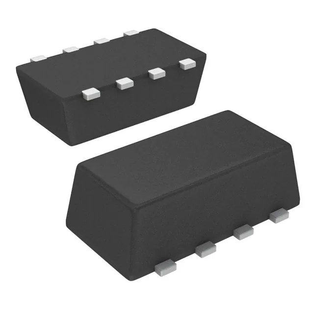
8-SMD, Flat Leads
Datasheet:
AetrixSI5441BDC-T1-E3.pdf
Description:
MOSFET P-CH 20V 4.4A 1206-8
Quantity:
Payment:
Payment
Shipping:
Shipping

Inventory:5,818

Please send an inquiry. Send us your inquiry, and we will respond immediately.

Part Number
Quantity*
Price
Name*
Company
Email*
Comments

Product details

Overview

SI5441BDC-T1-E3 from Vishay Siliconix is a P-channel enhancement-mode MOSFET designed for high-efficiency load switching in space-constrained DC-DC converters and power management circuits. It features -20 V VDS, 0.045 Ω RDS(on) at VGS = -4.5 V, -6.1 A continuous drain current, and a 1206-8 ChipFET® package optimized for thermal performance on compact PCBs.

For engineers reviewing the SI5441BDC-T1-E3 datasheet, SI5441BDC-T1-E3 pinout, SI5441BDC-T1-E3 application, or SI5441BDC-T1-E3 equivalent, key selection criteria include gate threshold voltage (-1.4 V typ), low gate charge (11.5 nC), junction-to-foot thermal resistance (17 °C/W), and compatibility with 2.5-V logic-level drive in battery-powered systems.

Technical Context

This device operates as a single-channel, surface-mount P-channel MOSFET with trench-based silicon architecture enabling low on-resistance and fast switching. Its gate threshold voltage range (-0.6 V to -1.4 V) supports reliable turn-on with 2.5–3.3 V control signals, while the integrated body diode (VSD = -0.8 to -1.2 V at -1.1 A) enables synchronous rectification and reverse-current blocking.

The 1206-8 ChipFET® package uses exposed drain terminals (pins 1,2,3,6,7,8) for direct thermal coupling to PCB copper, achieving 17 °C/W typical junction-to-foot resistance. Its leadless construction eliminates solder fillet dependency at terminal ends, relying instead on bottom-side solder interconnection across six drain pads and one source pad.

Key Specifications

ParameterValue and Actual Design Meaning
VDS-20 V - Maximum drain-source blocking voltage for 3.3 V rail protection and battery reverse-polarity circuits
RDS(on)0.045 Ω at VGS = -4.5 V - Enables <150 mW conduction loss at 6 A, critical for thermally limited handheld devices
ID (continuous)-6.1 A at TA = 25 °C - Supports high-current load switches without external heatsinking on standard FR4
Qg11.5 nC (typ) - Reduces gate drive power and switching transition time in 500 kHz–1 MHz DC-DC controllers
VGS(th)-1.4 V (typ) - Ensures full enhancement with 2.5 V logic outputs, eliminating need for level-shifting circuitry
RthJF17 °C/W (typ) - Delivers SO-8–class thermal performance in 80% smaller footprint via exposed drain thermal path
PD2.5 W at TA = 25 °C - Sustains >3 W pulsed power in short-duration load-dump or inrush scenarios

Pinout & Package

The SI5441BDC-T1-E3 is housed in a leadless 1206-8 ChipFET® package (JEDEC MS-012 variant), measuring 3.05 mm × 1.90 mm × 0.15 mm with six exposed drain terminals, one gate, and one source-designed for bottom-side reflow soldering and thermal conduction through PCB copper.

Pin/TerminalCircuit RoleDesign Meaning
1, 2, 3, 6, 7, 8 (Drain)Drain connection (6 parallel terminals)Collectively form low-inductance, high-current drain node; all must be connected to same net and thermal plane for rated RthJF
4 (Gate)Control electrodeReceives logic-level gate drive; requires <12 V absolute max rating and minimal trace inductance to avoid ringing
5 (Source)Reference node for gate drive and current returnServes as local ground reference for gate driver; must be low-impedance path to system ground to maintain VGS stability

Key Features

FeatureDesign Value
TrenchFET® technologyEnables 0.045 Ω RDS(on) in ultra-small 1206-8 footprint, reducing board area vs. SO-8 by 80% without sacrificing power handling
Leadless ChipFET® packageExposes six drain terminals directly to PCB for thermal conduction, achieving 17 °C/W junction-to-foot resistance comparable to SO-8
Low VGS(th) (-1.4 V typ)Guarantees full enhancement with 2.5 V microcontroller GPIO, eliminating gate driver ICs in portable battery systems
Halogen-free constructionMeets IEC 61249-2-21 compliance for environmentally restricted end equipment without compromising dielectric strength or thermal reliability
100% Rg testedEach unit verified for 10 Ω gate resistance, ensuring consistent switching speed and EMI profile across production lots

Applications

Battery Protection CircuitUSB Power Delivery Switch

Use Scenario: Reverse-polarity and overcurrent protection in single-cell Li-ion battery packs.

IC Role / Device Role / Timing Role: High-side P-channel switch controlling battery discharge path with fast fault response.

Use Value: -20 V VDS withstands load dump transients; 0.045 Ω RDS(on) limits voltage drop to <270 mV at 6 A, preserving runtime.

Use Scenario: Bidirectional power path control in USB-C PD sink applications requiring 5–20 V input switching.

IC Role / Device Role / Timing Role: Load switch enabling/disabling VBUS connection based on CC logic signaling.

Use Value: 11.5 nC Qg allows clean 10 µs turn-on/turn-off transitions under 3.3 V control, meeting USB PD timing requirements.

Point-of-Load DC-DC ConverterIndustrial Sensor Node Power Rail

Use Scenario: Synchronous rectifier in 3.3 V output buck converter for FPGA or DSP core supplies.

IC Role / Device Role / Timing Role: Low-side synchronous rectifier replacing Schottky diode to improve efficiency.

Use Value: Integrated body diode with -0.8 V VSD enables efficient freewheeling; low RDS(on) cuts conduction losses by >40% vs. discrete diode solution.

Use Scenario: Always-on power switch for wireless sensor nodes powered by coin-cell or energy-harvesting sources.

IC Role / Device Role / Timing Role: Ultra-low-quiescent-load enable switch isolating subsystems during sleep mode.

Use Value: -1 µA IDSS leakage at -20 V ensures <100 nA total off-state current, extending 10-year battery life targets.

Equivalent & Alternatives

The following parts are listed as comparable options for similar P-channel load switch applications.

Alternative PartTechnical DifferenceApplication DifferenceSelection Advice
Si5401DC-T1-E3-20 V VDS, 0.035 Ω RDS(on) at -4.5 V, but higher Qg (14.5 nC) and same 1206-8 packageBetter conduction loss at high current; slower switching due to higher gate chargeSelect when minimizing I²R loss dominates over switching frequency constraints
DMN2020LFG-7-20 V VDS, 0.042 Ω RDS(on) at -4.5 V, 8-pin WDFN (2×2 mm), no halogen-free certificationSmaller footprint (2×2 mm vs. 3.05×1.90 mm), but lower thermal mass and unverified halogen-free statusSelect when board area is critical and environmental compliance is not mandated

Compared with Si5401DC-T1-E3 and DMN2020LFG-7, the SI5441BDC-T1-E3 delivers optimal balance of low gate charge (11.5 nC), industry-standard halogen-free compliance, and proven thermal performance in the widely adopted 1206-8 footprint-making it preferred for cost-sensitive, high-volume portable electronics where reliability and supply chain continuity matter.

Availability

SI5441BDC-T1-E3 is available at Aetrix Electronics and suitable for battery protection circuits, USB power delivery switches, point-of-load DC-DC converters, and industrial sensor node power rails requiring stable component supply across multi-year production cycles.

Supply support for SI5441BDC-T1-E3 includes scheduled delivery planning, volume procurement assistance, BOM continuity management, traceable sourcing, and lifecycle availability coordination for OEM customers, industrial embedded developers, connected-device designers, and electronics production programs.

Manufacturer

Vishay Siliconix is a global leader in discrete semiconductors and passive components, specializing in high-reliability power MOSFETs, diodes, and resistors for automotive, industrial, and computing markets.

The Si5441BDC belongs to Vishay's TrenchFET® P-channel MOSFET product line, engineered specifically for high-efficiency, low-voltage load switching in space- and thermal-constrained portable electronics.

FAQ

What is the maximum continuous drain current rating for SI5441BDC-T1-E3 at 85 °C ambient temperature?

The SI5441BDC-T1-E3 supports -4.4 A continuous drain current at TA = 85 °C, derated from -6.1 A at 25 °C per its thermal resistance profile. This rating assumes proper PCB copper area per Vishay AN811 guidelines and accounts for steady-state junction temperature limits of 150 °C. The SI5441BDC-T1-E3 achieves this performance using its 1206-8 ChipFET® package's six-drain-terminal configuration to minimize RthJA.

Does SI5441BDC-T1-E3 support 2.5 V logic-level gate drive?

Yes, the SI5441BDC-T1-E3 has a typical gate threshold voltage of -1.4 V and guaranteed RDS(on) of 0.080 Ω at VGS = -2.5 V, enabling full enhancement with standard 2.5 V microcontroller outputs. Its trench-based design ensures robust turn-on even with marginal gate drive margins, making the SI5441BDC-T1-E3 suitable for battery-powered systems where supply voltage may sag below 3.0 V.

What is the thermal resistance from junction to foot (RthJF) for SI5441BDC-T1-E3, and why does it matter?

The SI5441BDC-T1-E3 has a typical junction-to-foot thermal resistance of 17 °C/W, measured from die junction to the exposed drain terminals. This parameter matters because it defines the dominant thermal path in compact layouts: heat flows directly from the silicon die into the PCB copper via the six drain pads, bypassing less efficient junction-to-ambient convection. Optimizing this path makes the SI5441BDC-T1-E3 viable in thermally dense designs where SO-8 packages would overheat.

Is SI5441BDC-T1-E3 halogen-free and RoHS-compliant?

Yes, the SI5441BDC-T1-E3 is both halogen-free per IEC 61249-2-21 and RoHS-compliant (Pb-free). The "-E3" suffix explicitly denotes lead-free and halogen-free construction, verified in Vishay's manufacturing process and documented in datasheet revision B. This compliance ensures suitability for consumer electronics and medical devices subject to strict environmental regulations, confirming the SI5441BDC-T1-E3 meets global market access requirements.

Can SI5441BDC-T1-E3 be used as a synchronous rectifier in a buck converter?

Yes, the SI5441BDC-T1-E3 is well-suited as a low-side synchronous rectifier in buck converters operating up to 1 MHz. Its 11.5 nC total gate charge enables fast turn-on/turn-off transitions, while its integrated body diode (VSD = -0.8 to -1.2 V) provides controlled freewheeling. When driven synchronously, the SI5441BDC-T1-E3 reduces conduction losses by >40% versus a Schottky diode, directly improving converter efficiency-especially at 3–5 A output currents.

SI5441BDC-T1-E3 Specifications

Product attributes
Attribute value
Manufacturer:
Vishay Siliconix
Series:
TrenchFET®
Package/Case:
8-SMD, Flat Leads
Packaging:
Tape & Reel (TR)
Product Status:
Obsolete
FET Type:
P-Channel
Technology:
MOSFET (Metal Oxide)
Drain to Source Voltage (Vdss):
20 V
Current - Continuous Drain (Id) @ 25°C:
4.4A (Ta)
Drive Voltage (Max Rds On, Min Rds On):
2.5V, 4.5V
Rds On (Max) @ Id, Vgs:
45mOhm @ 4.4A, 4.5V
Vgs(th) (Max) @ Id:
1.4V @ 250µA
Gate Charge (Qg) (Max) @ Vgs:
22 nC @ 4.5 V
Vgs (Max):
±12V
Input Capacitance (Ciss) (Max) @ Vds:
-
FET Feature:
-
Power Dissipation (Max):
1.3W (Ta)
Operating Temperature:
-55°C ~ 150°C (TJ)
Grade:
-
Qualification:
-
Mounting Type:
Surface Mount
Supplier Device Package:
1206-8 ChipFET™

SI5441BDC-T1-E3 FAQ

1.How can I place an order for SI5441BDC-T1-E3 through Aetrix?

Please submit a Request for Quotation (RFQ) for SI5441BDC-T1-E3 on Aetrix. Our sales agent will provide a competitive quotation and guide you through the order confirmation once you accept the terms.

2.Are the price and stock information for SI5441BDC-T1-E3 reliable?

The price and inventory of SI5441BDC-T1-E3 are updated periodically and may fluctuate due to market conditions. Stock and pricing data are typically refreshed every 24 hours. Quotation validity for SI5441BDC-T1-E3 is usually 5 days.

3.What payment methods are accepted for SI5441BDC-T1-E3?

We accept Wire Transfer, PayPal, Credit Card, Western Union, MoneyGram, and Escrow for SI5441BDC-T1-E3 transactions.

Note: Certain payment methods may incur a processing fee.

4.How is shipping managed for SI5441BDC-T1-E3?

SI5441BDC-T1-E3 orders can be shipped via leading logistics carriers, including DHL, UPS, FedEx, TNT, or Registered Mail.

Once your SI5441BDC-T1-E3 order is processed, you will receive an email with the shipment details and tracking number.

Note: Tracking information may take up to 24 hours to appear. Express delivery typically takes 3–5 business days.

5.How can I obtain technical support or documentation for SI5441BDC-T1-E3?

For technical support, including SI5441BDC-T1-E3 datasheets, pinout diagrams, or application guidance, please contact our engineering support team. They can provide detailed documentation and assistance for your SI5441BDC-T1-E3 requirements.

6.How does Aetrix verify that SI5441BDC-T1-E3 is sourced from the original manufacturer or authorized distributors?

All SI5441BDC-T1-E3 products on Aetrix are procured from qualified distributors and authorized channels. Our dedicated quality assurance team conducts strict verification, including traceability checks and, if necessary, third-party testing. This ensures that SI5441BDC-T1-E3 meets industry standards.

7.What is the process for return or replacement of SI5441BDC-T1-E3?

All SI5441BDC-T1-E3 units undergo pre-shipment inspection (PSI). If there is an issue with SI5441BDC-T1-E3, returns or replacements are accepted under the following conditions:

1.Quantity discrepancies, incorrect items, or visible external defects (such as breakage or corrosion), acknowledged by Aetrix.

2.The issue is reported within 90 days of delivery.

3.The SI5441BDC-T1-E3 part is unused and in its original packaging.

Return procedure for SI5441BDC-T1-E3:

1.Submit a request within 90 days.

2.Obtain a Return Material Authorization (RMA) from Aetrix.

SI5441BDC-T1-E3 Tags
  • SI5441BDC-T1-E3
  • SI5441BDC-T1-E3 PDF
  • SI5441BDC-T1-E3 Datasheet
  • SI5441BDC-T1-E3 Specifications
  • SI5441BDC-T1-E3 Images
  • Vishay Siliconix
  • Vishay Siliconix SI5441BDC-T1-E3
  • Buy SI5441BDC-T1-E3
  • SI5441BDC-T1-E3 Price
  • SI5441BDC-T1-E3 Distributor
  • SI5441BDC-T1-E3 Supplier
  • SI5441BDC-T1-E3 Wholesale
Related Products
BSZ180P03NS3EGATMA1
BSZ180P03NS3EGATMA1

Infineon Technologies
SIRA14DP-T1-GE3
SIRA14DP-T1-GE3

Vishay Siliconix

AO4419
AO4419

Alpha & Omega Semiconductor Inc.
SISA14BDN-T1-GE3
SISA14BDN-T1-GE3

Vishay Siliconix

PSMN9R5-30YLC,115
PSMN9R5-30YLC,115

Nexperia USA Inc.

BUK9Y21-40E,115
BUK9Y21-40E,115

Nexperia USA Inc.

RTQ035N03HZGTR
RTQ035N03HZGTR

Rohm Semiconductor

FDMS7680
FDMS7680

onsemi

RQ3E180BNTB
RQ3E180BNTB

Rohm Semiconductor

STL6N2VH5
STL6N2VH5

STMicroelectronics

DMPH4029LFGQ-7
DMPH4029LFGQ-7

Diodes Incorporated

DMT6015LSS-13
DMT6015LSS-13

Diodes Incorporated

Tech Hub

Search

Search

PRODUCT

PRODUCT

PHONE

PHONE

USER

USER