Send an Inquiry

To receive a quote for your project, please fill in the following information, and we’ll get back to you promptly.

Name*
Company*
Email Address*
Phone/WhatsApp
Part Number*
Quantity*
Message
Submit Inventory List

Please fill in the following information, and we’ll get back to you promptly.

Name*
Company*
Email Address*
Phone/WhatsApp
Upload My List
Message

Vishay Siliconix SI5475DC-T1-E3

Part No.:
SI5475DC-T1-E3
Manufacturer:
Vishay Siliconix
Category:
FETs, MOSFETs
Package:
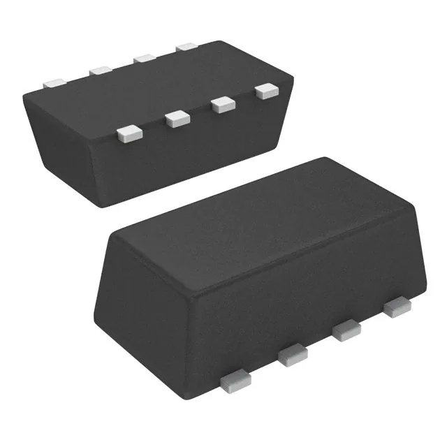
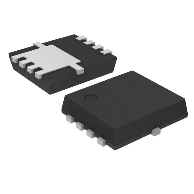
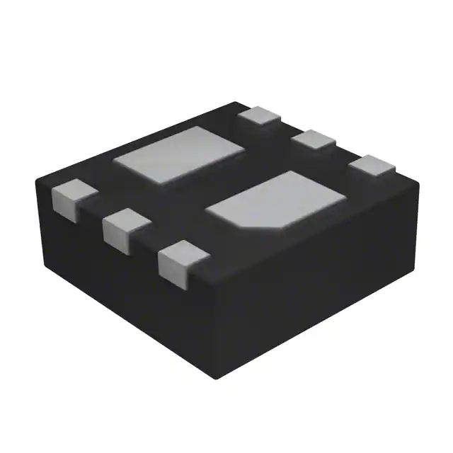
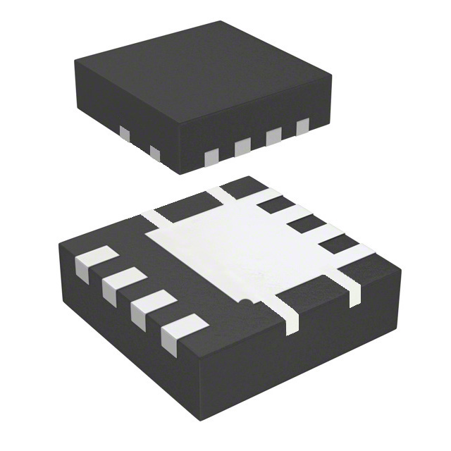
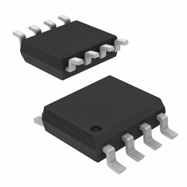
8-SMD, Flat Leads
Datasheet:
AetrixSI5475DC-T1-E3.pdf
Description:
MOSFET P-CH 12V 5.5A 1206-8
Quantity:
Payment:
Payment
Shipping:
Shipping

Inventory:8,924

Please send an inquiry. Send us your inquiry, and we will respond immediately.

Part Number
Quantity*
Price
Name*
Company
Email*
Comments

Product details

Overview

SI5475DC-T1-E3 from Vishay Siliconix is a P-channel enhancement-mode TrenchFET® MOSFET rated for -12 V drain-source voltage, with 0.031 Ω RDS(on) at VGS = -4.5 V and -5.5 A continuous drain current at 25 °C. It features 1.8 V gate threshold compatibility, halogen-free construction per IEC 61249-2-21, and is optimized for low-voltage load switching in space-constrained DC-DC converters and battery protection circuits.

For engineers reviewing the SI5475DC-T1-E3 datasheet, SI5475DC-T1-E3 pinout, SI5475DC-T1-E3 application, or SI5475DC-T1-E3 equivalent, key selection criteria include its 1206-8 ChipFET package, -1.8 V gate drive capability, junction-to-foot thermal resistance of 15–20 °C/W, and verified performance under pulsed drain currents up to ±20 A.

Technical Context

This device operates as a single P-channel power switch with a negative gate threshold voltage (-0.45 V typical) and integrated body diode (VSD = -0.7 to -1.2 V at -1.1 A). Its trench-based silicon structure enables low on-resistance while maintaining stable transconductance (19 S typical) and fast switching dynamics (td(off) = 122–180 ns).

The SI5475DC-T1-E3 is designed for surface-mount operation on FR4 boards with no requirement for solder fillets at exposed copper terminations. Thermal management relies on direct heat conduction through the drain pad to PCB copper, supported by a steady-state RthJA of 80–95 °C/W and RthJF of 15–20 °C/W.

Key Specifications

ParameterValue and Actual Design Meaning
VDS-12 V - Maximum blocking voltage for low-side or high-side switching in ≤12 V systems
RDS(on)0.031 Ω at VGS = -4.5 V - Enables <170 mW conduction loss at 5.5 A, critical for thermally limited layouts
ID (continuous)-5.5 A at TA = 25 °C - Supports sustained load switching in compact 1206-8 footprint without forced airflow
VGS(th)-0.45 V typical - Ensures reliable turn-on with 1.8 V logic-level control, eliminating need for level shifters
Qg19–29 nC - Low gate charge reduces driver power demand and switching losses in high-frequency PWM
RthJF15–20 °C/W - Efficient heat transfer from junction to PCB foot enables higher power density than standard SO-8 equivalents
VSD-0.7 to -1.2 V - Body diode forward voltage supports synchronous rectification or reverse-polarity protection

Pinout & Package

SI5475DC-T1-E3 uses the 1206-8 ChipFET package: a leadless, bottom-terminal surface-mount design measuring 3.0 mm × 1.8 mm with exposed drain pads on the underside. The top marking "BF" identifies the part family and lot traceability code.

Pin/TerminalCircuit RoleDesign Meaning
D (Drain)Main current path output / heat sink nodeEight exposed copper terminals on bottom side form parallel drain connections; primary thermal path to PCB
G (Gate)Control inputSingle top-side pad; requires clean 1.8–4.5 V negative-going signal for full enhancement
S (Source)Reference return / current return pathTop-side pad; connects to system ground or battery negative in high-side configurations

Key Features

FeatureDesign Value
TrenchFET® architectureEnables 0.031 Ω RDS(on) in 3.0 mm × 1.8 mm footprint-reducing board area vs. SO-8 by >65%
1.8 V gate ratingGuarantees full enhancement with standard 1.8 V microcontroller GPIO, eliminating external level-shifting circuitry
Halogen-free & RoHS-compliantMeets IEC 61249-2-21 and Directive 2002/95/EC-enabling use in consumer, industrial, and automotive supply chains
Exposed drain thermal padProvides 15–20 °C/W junction-to-foot resistance-enabling 2.5 W dissipation on 1" × 1" FR4 without heatsink
Low Qgd/Qg ratio3.6/19–29 nC ratio improves Miller immunity and enables stable switching at >1 MHz in buck converters

Applications

Battery Protection CircuitUSB Power Switch

Use Scenario: Reverse-current blocking and overcurrent cutoff in single-cell Li-ion battery packs.

IC Role / Device Role / Timing Role: P-channel MOSFET used as high-side protection switch controlled by battery management IC.

Use Value: 1.8 V gate threshold allows direct interface with low-voltage BMS outputs; 0.031 Ω RDS(on) limits voltage drop to <170 mV at 5.5 A, preserving pack efficiency.

Use Scenario: Hot-swap power control for USB 2.0/3.0 downstream ports in portable hubs and docking stations.

IC Role / Device Role / Timing Role: Load switch isolating VBUS during insertion/removal to prevent inrush and bus contention.

Use Value: Fast 122–180 ns turn-off delay prevents glitch propagation; halogen-free construction satisfies USB-IF environmental compliance requirements.

DC-DC Converter Synchronous RectifierIndustrial Sensor Node Power Gate

Use Scenario: Secondary-side synchronous rectification in isolated 5 V–12 V flyback converters for IoT gateways.

IC Role / Device Role / Timing Role: P-channel switch replacing Schottky diode to reduce conduction loss and improve efficiency.

Use Value: -1.2 V VSD and low Qg enable efficient operation at 300–500 kHz; RthJF of 15–20 °C/W sustains 2.5 W dissipation in sealed enclosures.

Use Scenario: Controlled power gating of analog sensor front-ends and RF transceivers in battery-powered condition monitoring nodes.

IC Role / Device Role / Timing Role: Low-quiescent-power load switch enabling deep-sleep mode with <1 µA off-state leakage.

Use Value: -1 µA IDSS at -9.6 V ensures <100 nA system standby current; 1206-8 footprint fits within 8 mm² PCB area budgets.

Equivalent & Alternatives

The following parts are listed as comparable options for similar P-channel MOSFET applications.

Alternative PartTechnical DifferenceApplication DifferenceSelection Advice
Si7157DP-T1-GE3-20 V VDS, 0.022 Ω RDS(on) at -4.5 V, 8-A ID, PowerPAK® 1212-8 packageHigher voltage rating and lower on-resistance, but larger 3.2 mm × 3.2 mm footprintSelect when ≥20 V blocking or <0.025 Ω RDS(on) is required; verify PCB layout compatibility with larger thermal pad
DMG1012T-7-12 V VDS, 0.045 Ω RDS(on) at -4.5 V, 4.5-A ID, SOT-563 packageSmaller SOT-563 footprint but higher RDS(on) and lower current ratingSelect when board space is more constrained than thermal budget; confirm 0.045 Ω loss acceptable at target load current

Compared with Si7157DP-T1-GE3 and DMG1012T-7, the SI5475DC-T1-E3 delivers optimal balance of 12 V rating, 0.031 Ω on-resistance, and minimal 3.0 mm × 1.8 mm footprint-making it preferred for space-limited 5–12 V load switching where thermal headroom is moderate.

Availability

SI5475DC-T1-E3 is available at Aetrix Electronics and suitable for battery protection circuits, USB power switches, DC-DC converter synchronous rectifiers, and industrial sensor node power gates requiring stable component supply across production lifecycles.

Supply support for SI5475DC-T1-E3 includes scheduled delivery planning, volume procurement assistance, BOM continuity management, traceable sourcing, and lifecycle availability coordination for OEM customers, industrial embedded developers, connected-device designers, and electronics production programs.

Manufacturer

Vishay Siliconix is a global leader in discrete semiconductors, specializing in MOSFETs, diodes, optoelectronics, and passive components with emphasis on power efficiency, reliability, and miniaturization.

The SI5475DC-T1-E3 belongs to Vishay's TrenchFET® P-channel MOSFET product line, engineered specifically for high-efficiency, low-voltage load switching in space-constrained portable and industrial electronics.

FAQ

What is the maximum continuous drain current for SI5475DC-T1-E3 at 85 °C ambient temperature?

The SI5475DC-T1-E3 supports -3.5 A continuous drain current at TA = 85 °C, as specified in the Absolute Maximum Ratings table. This derating reflects thermal limitations of the 1206-8 ChipFET package under natural convection on standard FR4. For higher current operation at elevated ambient, PCB copper area and thermal vias must be optimized to maintain junction temperature below 150 °C. The SI5475DC-T1-E3 datasheet confirms this value under steady-state conditions with no forced airflow.

Does SI5475DC-T1-E3 require a gate resistor for stable switching in a 500 kHz DC-DC converter?

The SI5475DC-T1-E3 benefits from a small gate resistor (typically 2.2–10 Ω) to damp ringing and control dV/dt, especially given its 3.6 nC Qgd and low 19–29 nC Qg. While not strictly required for functionality, a series gate resistor improves EMI performance and prevents shoot-through in half-bridge configurations. The SI5475DC-T1-E3's fast 15–25 ns turn-on delay and 80–120 ns fall time make controlled edge rates essential at 500 kHz switching frequencies.

Can SI5475DC-T1-E3 be used in a high-side configuration with 3.3 V logic control?

No-SI5475DC-T1-E3 is a P-channel MOSFET requiring a negative gate-to-source voltage for enhancement. With a 3.3 V logic high, the gate would sit at 3.3 V while the source is at VIN (e.g., 5 V), resulting in VGS = -1.7 V, which is insufficient for full turn-on (RDS(on) rises sharply below -2.5 V). To drive SI5475DC-T1-E3 in high-side mode, a dedicated gate driver or charge pump generating ≥-4.5 V relative to source is required. Direct 3.3 V logic control only works in low-side configurations.

What is the peak pulsed drain current rating for SI5475DC-T1-E3, and under what conditions is it valid?

The SI5475DC-T1-E3 has a peak pulsed drain current rating of ±20 A, defined for pulse widths ≤300 µs and duty cycles ≤2 % at TJ = 25 °C. This rating assumes adequate PCB copper mass to absorb transient energy without exceeding the 150 °C maximum junction temperature. It is not sustainable under DC or high-duty-cycle conditions-the SI5475DC-T1-E3's continuous rating remains -5.5 A at 25 °C ambient. Pulse testing follows JEDEC JESD24-1 guidelines.

Is SI5475DC-T1-E3 compatible with lead-free reflow profiles per IPC/JEDEC J-STD-020?

Yes-SI5475DC-T1-E3 is qualified for lead-free reflow with a peak temperature of 260 °C, compliant with IPC/JEDEC J-STD-020 Class 3 moisture sensitivity level (MSL) requirements. The device is marked "T1-E3" to indicate lead-free (Pb-free) termination and conforms to RoHS Directive 2002/95/EC. No pre-bake is required for standard MSL handling, but storage per J-STD-033 guidelines is recommended for humidity-sensitive packaging.

SI5475DC-T1-E3 Specifications

Product attributes
Attribute value
Manufacturer:
Vishay Siliconix
Series:
TrenchFET®
Package/Case:
8-SMD, Flat Leads
Packaging:
Tape & Reel (TR)
Product Status:
Obsolete
FET Type:
P-Channel
Technology:
MOSFET (Metal Oxide)
Drain to Source Voltage (Vdss):
12 V
Current - Continuous Drain (Id) @ 25°C:
5.5A (Ta)
Drive Voltage (Max Rds On, Min Rds On):
1.8V, 4.5V
Rds On (Max) @ Id, Vgs:
31mOhm @ 5.5A, 4.5V
Vgs(th) (Max) @ Id:
450mV @ 1mA (Min)
Gate Charge (Qg) (Max) @ Vgs:
29 nC @ 4.5 V
Vgs (Max):
±8V
Input Capacitance (Ciss) (Max) @ Vds:
-
FET Feature:
-
Power Dissipation (Max):
1.3W (Ta)
Operating Temperature:
-55°C ~ 150°C (TJ)
Grade:
-
Qualification:
-
Mounting Type:
Surface Mount
Supplier Device Package:
1206-8 ChipFET™

SI5475DC-T1-E3 FAQ

1.How can I place an order for SI5475DC-T1-E3 through Aetrix?

Please submit a Request for Quotation (RFQ) for SI5475DC-T1-E3 on Aetrix. Our sales agent will provide a competitive quotation and guide you through the order confirmation once you accept the terms.

2.Are the price and stock information for SI5475DC-T1-E3 reliable?

The price and inventory of SI5475DC-T1-E3 are updated periodically and may fluctuate due to market conditions. Stock and pricing data are typically refreshed every 24 hours. Quotation validity for SI5475DC-T1-E3 is usually 5 days.

3.What payment methods are accepted for SI5475DC-T1-E3?

We accept Wire Transfer, PayPal, Credit Card, Western Union, MoneyGram, and Escrow for SI5475DC-T1-E3 transactions.

Note: Certain payment methods may incur a processing fee.

4.How is shipping managed for SI5475DC-T1-E3?

SI5475DC-T1-E3 orders can be shipped via leading logistics carriers, including DHL, UPS, FedEx, TNT, or Registered Mail.

Once your SI5475DC-T1-E3 order is processed, you will receive an email with the shipment details and tracking number.

Note: Tracking information may take up to 24 hours to appear. Express delivery typically takes 3–5 business days.

5.How can I obtain technical support or documentation for SI5475DC-T1-E3?

For technical support, including SI5475DC-T1-E3 datasheets, pinout diagrams, or application guidance, please contact our engineering support team. They can provide detailed documentation and assistance for your SI5475DC-T1-E3 requirements.

6.How does Aetrix verify that SI5475DC-T1-E3 is sourced from the original manufacturer or authorized distributors?

All SI5475DC-T1-E3 products on Aetrix are procured from qualified distributors and authorized channels. Our dedicated quality assurance team conducts strict verification, including traceability checks and, if necessary, third-party testing. This ensures that SI5475DC-T1-E3 meets industry standards.

7.What is the process for return or replacement of SI5475DC-T1-E3?

All SI5475DC-T1-E3 units undergo pre-shipment inspection (PSI). If there is an issue with SI5475DC-T1-E3, returns or replacements are accepted under the following conditions:

1.Quantity discrepancies, incorrect items, or visible external defects (such as breakage or corrosion), acknowledged by Aetrix.

2.The issue is reported within 90 days of delivery.

3.The SI5475DC-T1-E3 part is unused and in its original packaging.

Return procedure for SI5475DC-T1-E3:

1.Submit a request within 90 days.

2.Obtain a Return Material Authorization (RMA) from Aetrix.

SI5475DC-T1-E3 Tags
  • SI5475DC-T1-E3
  • SI5475DC-T1-E3 PDF
  • SI5475DC-T1-E3 Datasheet
  • SI5475DC-T1-E3 Specifications
  • SI5475DC-T1-E3 Images
  • Vishay Siliconix
  • Vishay Siliconix SI5475DC-T1-E3
  • Buy SI5475DC-T1-E3
  • SI5475DC-T1-E3 Price
  • SI5475DC-T1-E3 Distributor
  • SI5475DC-T1-E3 Supplier
  • SI5475DC-T1-E3 Wholesale
Related Products
BSZ180P03NS3EGATMA1
BSZ180P03NS3EGATMA1

Infineon Technologies
SIRA14DP-T1-GE3
SIRA14DP-T1-GE3

Vishay Siliconix

AO4419
AO4419

Alpha & Omega Semiconductor Inc.
SISA14BDN-T1-GE3
SISA14BDN-T1-GE3

Vishay Siliconix

PSMN9R5-30YLC,115
PSMN9R5-30YLC,115

Nexperia USA Inc.

BUK9Y21-40E,115
BUK9Y21-40E,115

Nexperia USA Inc.

RTQ035N03HZGTR
RTQ035N03HZGTR

Rohm Semiconductor

FDMS7680
FDMS7680

onsemi

RQ3E180BNTB
RQ3E180BNTB

Rohm Semiconductor

STL6N2VH5
STL6N2VH5

STMicroelectronics

DMPH4029LFGQ-7
DMPH4029LFGQ-7

Diodes Incorporated

DMT6015LSS-13
DMT6015LSS-13

Diodes Incorporated

Tech Hub

Search

Search

PRODUCT

PRODUCT

PHONE

PHONE

USER

USER