
 My Inquiry
 My Account


onsemi SMDA05-6R2
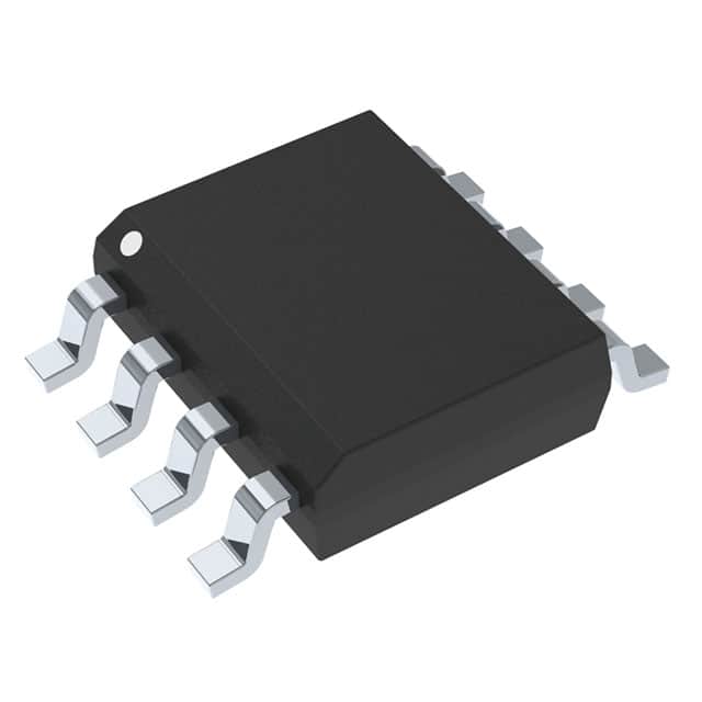
- Part No.:
- SMDA05-6R2
- Manufacturer:
- onsemi
- Category:
- TVS Diodes
- Package:
- 8-SOIC (0.154", 3.90mm Width)
- Datasheet:
-
 SMDA05-6R2.pdf
- Description:
- TVS DIODE 5VWM 11VC 8-SOIC
- Quantity:
- Payment:

- Shipping:

Inventory:2,581
Please send an inquiry. Send us your inquiry, and we will respond immediately.
Product details
Overview
SMDA05-6R2 from onsemi is a unidirectional transient voltage suppressor (TVS) array in SO-8 package, designed for ESD/EFT/lightning protection of up to six high-speed data lines. It features 6.0 V breakdown voltage, 400 W peak pulse power (8 × 20 µs), 17 A peak pulse current, 9.8 V clamping voltage at 1.0 A, and IEC 61000-4-2 ±15 kV (air)/±8 kV (contact) rating - deployed in LAN/WAN equipment and microprocessor I/O protection.
For engineers reviewing the SMDA05-6R2 datasheet, pinout, applications, or equivalent options, key selection criteria include its 6 V working voltage, cathode-anode pin mapping across eight terminals, unidirectional polarity, 20 µA max reverse leakage at 5.0 V, and UL 94 V-0 flammability compliance for board-level safety certification.
Technical Context
The SMDA05-6R2 integrates six independent unidirectional TVS diodes in a single SO-8 package, with pins 1–5 and 8 as cathodes and pins 6–7 as anodes - enabling discrete line protection without external routing. Its 6.0 V reverse breakdown ensures compatibility with 5.0 V logic systems while maintaining low clamping (≤9.8 V @ 1 A) to safeguard downstream transceivers.
It meets IEC 61000-4-4 (40 A EFT), IEC 61000-4-5 (12 A lightning surge), and IEC 61000-4-2 ESD standards, operating across −55 °C to +150 °C junction temperature. The device uses silicon avalanche technology with non-repetitive 8 × 20 µs pulse handling and 260 °C solder tolerance per JEDEC J-STD-020.
Key Specifications
| Parameter | Value and Actual Design Meaning |
|---|---|
| Breakdown Voltage | 6.0 V min @ 1.0 mA - ensures reliable turn-on before 5.0 V system rails exceed safe margins |
| Clamping Voltage | 9.8 V max @ 1.0 A - limits transient overvoltage to levels compatible with 3.3/5.0 V interface ICs |
| Peak Pulse Power | 400 W @ 8 × 20 µs - sustains high-energy surges without thermal runaway |
| Peak Pulse Current | 17 A @ 8 × 20 µs - supports robust lightning strike immunity per IEC 61000-4-5 |
| ESD Rating | ±15 kV air / ±8 kV contact per IEC 61000-4-2 - exceeds industrial ESD immunity requirements |
| Reverse Leakage | 20 µA max @ 5.0 V - minimizes standby power loss and signal distortion on idle lines |
Pinout & Package
SO-8 package (Case 751-07), 4.80–5.00 mm × 3.80–4.00 mm body, 1.27 mm pitch, 1.35–1.75 mm height, lead-free and RoHS-compliant.
| Pin/Terminal | Circuit Role | Design Meaning |
|---|---|---|
| 1 | Cathode | Protected line 1 cathode connection - ties to 5.0 V rail or ground-referenced clamp path |
| 2 | Cathode | Protected line 2 cathode connection - enables independent clamping per differential pair leg |
| 3 | Cathode | Protected line 3 cathode connection - supports multi-line USB or PCIe lane protection |
| 4 | Cathode | Protected line 4 cathode connection - used in parallel with adjacent cathodes for shared return |
| 5 | Cathode | Protected line 5 cathode connection - allows five dedicated cathode paths for asymmetric layouts |
| 6 | Anode | Common anode for lines 1–5 - connects to system ground or low-impedance return plane |
| 7 | Anode | Common anode for line 6 - isolated anode path enables sixth line with separate grounding |
| 8 | Cathode | Protected line 6 cathode connection - completes full six-line unidirectional protection set |
Key Features
| Feature | Design Value |
|---|---|
| Unidirectional 6-line array | Enables selective clamping on positive transients only - preserves DC bias integrity on 5.0 V data buses |
| 400 W peak pulse power | Handles repeated 8 × 20 µs surges without parameter shift - validated for industrial environment longevity |
| IEC 61000-4-2/4/5 compliance | Meets full immunity suite for EN 61000-6-2/6-4 - eliminates need for supplemental protection stages |
| UL 94 V-0 flammability rating | Prevents flame propagation during catastrophic failure - required for ITE and networking equipment safety approvals |
| SO-8 surface-mount package | Supports automated placement and reflow; footprint matches standard SOIC-8 land patterns for layout reuse |
Applications
| Ethernet PHY Protection | USB 2.0 Data Line Protection |
|---|---|
Use Scenario: Protecting 10/100/1000BASE-T Ethernet PHY interfaces against ESD events during cable hot-plug and lightning-induced surges. IC Role / Device Role / Timing Role: Unidirectional TVS array clamping each MDI pair (TX+/TX−, RX+/RX−) and auxiliary control lines. Use Value: Maintains signal integrity with ≤9.8 V clamping at 1 A while supporting >100 MHz bandwidth via low capacitance design. | Use Scenario: Safeguarding USB 2.0 D+ and D− lines in host controllers and peripheral devices against contact ESD up to ±8 kV. IC Role / Device Role / Timing Role: Six-channel TVS providing dedicated cathode/anode paths for D+, D−, VBUS, ID, and two sideband signals. Use Value: Prevents latch-up and damage to USB transceivers without adding series impedance or degrading eye diagram margin. |
| Server Management Interface | Industrial CAN Bus Node |
Use Scenario: Securing IPMI, SMBus, or PMBus lines connecting baseboard management controllers (BMC) to sensors and power modules. IC Role / Device Role / Timing Role: Low-leakage (≤20 µA) TVS protecting bidirectional 3.3 V/5.0 V management bus lines from board-handling ESD. Use Value: Ensures firmware update reliability and sensor readout accuracy by limiting transient overshoot to <10 V. | Use Scenario: Adding secondary surge protection to CAN_H/CAN_L plus VCC, GND, and enable lines in automotive-grade gateways. IC Role / Device Role / Timing Role: Unidirectional clamping on all six lines - leveraging pin 6/7 anodes for split-ground referencing in noisy chassis environments. Use Value: Complements primary CAN transceiver protection with 17 A surge capacity and −55 °C to +150 °C operation. |
Equivalent & Alternatives
The following parts are listed as comparable options for similar TVS array applications.
| Alternative Part | Technical Difference | Application Difference | Selection Advice |
|---|---|---|---|
| SMAJ5.0A | Single-channel, DO-214AC package, 5.0 V VBR, 400 W Ppk - lacks integrated multi-line configuration | Requires six discrete placements and routing - increases PCB area and parasitic inductance | Choose when board space permits discrete layout and tighter VBR tolerance (5.0 V vs. 6.0 V) is critical |
| SP1003-06UTG | 6-channel unidirectional array in SOT-23-6, 5.5 V VBR, 150 W Ppk - lower power rating and smaller package | Rated for 12 A IPP only - insufficient for IEC 61000-4-5 lightning testing at full severity | Choose for portable electronics where size and cost outweigh surge margin requirements |
Compared with SMAJ5.0A and SP1003-06UTG, the SMDA05-6R2 uniquely delivers six-line integration, 400 W surge capacity, and SO-8 manufacturability - making it optimal for fixed infrastructure requiring certified IEC 61000-4-5 immunity and production scalability.
Availability
SMDA05-6R2 is available at Aetrix Electronics and suitable for LAN/WAN equipment, server I/O protection, and industrial microprocessor-based systems requiring stable component supply and long-term lifecycle support.
Supply support for SMDA05-6R2 includes scheduled delivery planning, volume procurement assistance, BOM continuity management, traceable sourcing, and lifecycle availability coordination for OEM customers, industrial embedded developers, connected-device designers, and electronics production programs.
Manufacturer
onsemi (formerly ON Semiconductor) is a global semiconductor supplier delivering energy-efficient, intelligent power and sensing solutions for automotive, industrial, cloud, and IoT applications.
The SMDA05-6R2 belongs to onsemi's transient voltage suppression portfolio, engineered specifically for high-speed data line protection in networking, computing, and instrumentation systems where ESD robustness and compact integration are critical.
FAQ
What is the breakdown voltage specification for the SMDA05-6R2?
The SMDA05-6R2 has a minimum reverse breakdown voltage (VBR) of 6.0 V at 1.0 mA test current, measured per the device's electrical characteristics table. This value ensures consistent clamping onset above standard 5.0 V logic rails while avoiding false triggering during normal operation. The SMDA05-6R2 maintains this specification across its full operating temperature range of −55 °C to +150 °C.
How many protected lines does the SMDA05-6R2 support, and how are they configured?
The SMDA05-6R2 supports six independent high-speed data lines using a unidirectional architecture. Pins 1–5 and 8 serve as cathodes for individual lines, while pins 6 and 7 function as common anodes - allowing flexible grounding schemes. This configuration is explicitly defined in the "PIN CONFIGURATION AND SCHEMATIC" section of the official SMDA05-6R2 datasheet.
Does the SMDA05-6R2 meet international ESD and surge immunity standards?
Yes, the SMDA05-6R2 is rated per IEC 61000-4-2 (±15 kV air, ±8 kV contact), IEC 61000-4-4 (40 A EFT), and IEC 61000-4-5 (12 A lightning, 8/20 µs). These certifications are verified in the "Features" and "ELECTRICAL CHARACTERISTICS" sections of the SMDA05-6R2 datasheet and confirm suitability for EN 61000-6-2/6-4 compliance testing.
What is the maximum clamping voltage of the SMDA05-6R2 under surge conditions?
The SMDA05-6R2 exhibits a maximum clamping voltage (VC) of 9.8 V at 1.0 A and 11 V at 5.0 A, both measured with an 8 × 20 µs pulse waveform. These values define the upper voltage limit imposed on protected lines during transient events and are critical for ensuring compatibility with 3.3 V and 5.0 V interface ICs downstream of the SMDA05-6R2.
Is the SMDA05-6R2 compatible with standard SO-8 PCB footprints and reflow profiles?
Yes, the SMDA05-6R2 uses the industry-standard SO-8 package (Case 751-07) with 1.27 mm pitch and JEDEC-compliant dimensions. It supports lead-free reflow with a maximum lead solder temperature of 260 °C for 10 seconds, matching IPC/JEDEC J-STD-020 requirements. The SMDA05-6R2's land pattern and thermal profile are fully compatible with automated assembly lines using standard SOIC-8 tooling.
SMDA05-6R2 Specifications
- Product attributes
- Attribute value
- Manufacturer:
- onsemi
- Package/Case:
- 8-SOIC (0.154", 3.90mm Width)
- Series:
- -
- Packaging:
- Tape & Reel (TR)
- Product Status:
- Obsolete
- Type:
- Zener
- Unidirectional Channels:
- 6
- Bidirectional Channels:
- -
- Voltage - Reverse Standoff (Typ):
- 5V
- Voltage - Breakdown (Min):
- 6V
- Voltage - Clamping (Max) @ Ipp:
- 11V
- Current - Peak Pulse (10/1000µs):
- 17A (8/20µs)
- Power - Peak Pulse:
- 400W
- Power Line Protection:
- No
- Applications:
- General Purpose
- Capacitance @ Frequency:
- -
- Operating Temperature:
- -55°C ~ 150°C (TJ)
- Grade:
- -
- Qualification:
- -
- Mounting Type:
- Surface Mount
- Supplier Device Package:
- 8-SOIC
SMDA05-6R2 FAQ
1.How can I place an order for SMDA05-6R2 through Aetrix?
Please submit a Request for Quotation (RFQ) for SMDA05-6R2 on Aetrix. Our sales agent will provide a competitive quotation and guide you through the order confirmation once you accept the terms.
2.Are the price and stock information for SMDA05-6R2 reliable?
The price and inventory of SMDA05-6R2 are updated periodically and may fluctuate due to market conditions. Stock and pricing data are typically refreshed every 24 hours. Quotation validity for SMDA05-6R2 is usually 5 days.
3.What payment methods are accepted for SMDA05-6R2?
We accept Wire Transfer, PayPal, Credit Card, Western Union, MoneyGram, and Escrow for SMDA05-6R2 transactions.
Note: Certain payment methods may incur a processing fee.
4.How is shipping managed for SMDA05-6R2?
SMDA05-6R2 orders can be shipped via leading logistics carriers, including DHL, UPS, FedEx, TNT, or Registered Mail.
Once your SMDA05-6R2 order is processed, you will receive an email with the shipment details and tracking number.
Note: Tracking information may take up to 24 hours to appear. Express delivery typically takes 3–5 business days.
5.How can I obtain technical support or documentation for SMDA05-6R2?
For technical support, including SMDA05-6R2 datasheets, pinout diagrams, or application guidance, please contact our engineering support team. They can provide detailed documentation and assistance for your SMDA05-6R2 requirements.
6.How does Aetrix verify that SMDA05-6R2 is sourced from the original manufacturer or authorized distributors?
All SMDA05-6R2 products on Aetrix are procured from qualified distributors and authorized channels. Our dedicated quality assurance team conducts strict verification, including traceability checks and, if necessary, third-party testing. This ensures that SMDA05-6R2 meets industry standards.
7.What is the process for return or replacement of SMDA05-6R2?
All SMDA05-6R2 units undergo pre-shipment inspection (PSI). If there is an issue with SMDA05-6R2, returns or replacements are accepted under the following conditions:
1.Quantity discrepancies, incorrect items, or visible external defects (such as breakage or corrosion), acknowledged by Aetrix.
2.The issue is reported within 90 days of delivery.
3.The SMDA05-6R2 part is unused and in its original packaging.
Return procedure for SMDA05-6R2:
1.Submit a request within 90 days.
2.Obtain a Return Material Authorization (RMA) from Aetrix.
SMDA05-6R2 Tags
-
ESD9B5.0ST5G
onsemi
-
DESD3V3E1BL-7B
Diodes Incorporated
-
ESD5Z3.3T1G
onsemi
-
D5V0H1B2LP-7B
Diodes Incorporated
-
D5V0P1B2LP-7B
Diodes Incorporated
-
DESD5V0U1BA-7
Diodes Incorporated
-
ESD5Z5.0T1G
onsemi
-
DESD5V0U1BB-7
Diodes Incorporated
-
D12V0L1B2LP-7B
Diodes Incorporated
-
PESD2V0Y1BSFYL
Nexperia USA Inc.
-
DF2S5M4CT,L3F
Toshiba Semiconductor and Storage
-
D5V0L1B2WS-7
Diodes Incorporated
Tech Hub

Counterfeit components can hide behind convincing markings and passing basic function tests. This engineering reference covers source traceability, external inspection, X-ray, XRF, electrical testing, …

A practical engineering and sourcing framework covering lifecycle verification, lifetime-buy calculations, replacement qualification, supplier checks and counterfeit-risk controls.

TTL and CMOS logic families differ in thresholds, loading, output drive, power and timing. This engineering guide compares 74HC and 74HCT, calculates noise margins and checks 3.3 V/5 V compatibility.

A practical engineering guide to 3.3V and 5V logic compatibility, input thresholds, resistor dividers, translator ICs, MOSFET level shifting, I2C pull-ups, timing limits and power-sequencing risks.

The 74HC595 uses push-pull logic outputs, while the TPIC6B595 uses 50 V open-drain DMOS sinks for higher-power loads. This guide compares timing, current limits, 3.3 V interfacing, load wiring, thermal…

The 74HC595 converts serial data into eight stable parallel outputs. This guide covers pin functions, shift and storage timing, OE and MR behavior, drive-current limits, cascading, voltage compatibilit…

A technical comparison of level-sensitive latches and edge-triggered flip-flops, covering timing windows, setup and hold limits, master–slave operation, time borrowing, race-through, HDL inference and…

A D latch stores one bit while Enable controls when data can pass. This reference covers gate-level operation, truth tables, transparency, setup and hold timing, LE versus OE, common ICs and practical …

An SR latch stores one bit through cross-coupled feedback. This engineering reference covers NOR and NAND implementations, truth tables, forbidden-state recovery, gated operation, switch debouncing, fa…

Latch circuits retain one bit through feedback. This technical reference covers SR and D latches, truth tables, transparency, timing limits, latch-versus-flip-flop behavior, applications and common log…


