Send an Inquiry

To receive a quote for your project, please fill in the following information, and we’ll get back to you promptly.

Name*
Company*
Email Address*
Phone/WhatsApp
Part Number*
Quantity*
Message
Submit Inventory List

Please fill in the following information, and we’ll get back to you promptly.

Name*
Company*
Email Address*
Phone/WhatsApp
Upload My List
Message

Vishay Siliconix SQJ166ELP-T1_GE3

Part No.:
SQJ166ELP-T1_GE3
Manufacturer:
Vishay Siliconix
Category:
FETs, MOSFETs
Package:
PowerPAK® SO-8
Datasheet:
AetrixSQJ166ELP-T1_GE3.pdf
Description:
MOSFET N-CH 50V 50A TO252AA
Quantity:
Payment:
Payment
Shipping:
Shipping

Inventory:9,906

Please send an inquiry. Send us your inquiry, and we will respond immediately.

Part Number
Quantity*
Price
Name*
Company
Email*
Comments

Product details

Overview

SQJ166ELP-T1_GE3 from Vishay Siliconix is an automotive-grade N-channel 60 V MOSFET in PowerPAK® SO-8L package, delivering RDS(on) = 9.7 mΩ at VGS = 10 V and 15.0 mΩ at VGS = 4.5 V, rated for continuous drain current up to 67 A at TC = 25 °C, and qualified to AEC-Q101 for under-hood powertrain and body control modules.

For engineers reviewing the SQJ166ELP-T1_GE3 datasheet, SQJ166ELP-T1_GE3 pinout, SQJ166ELP-T1_GE3 application, or SQJ166ELP-T1_GE3 equivalent, this page delivers verified thermal resistance (RthJC = 1.68 °C/W), gate charge (Qg = 19–29 nC), avalanche energy rating (EAS = 24 mJ), and bottom-side thermal pad layout guidance per Vishay Doc. #78020.

Technical Context

This TrenchFET® Gen IV MOSFET uses optimized trench gate architecture to achieve low RDS(on) with high ruggedness, supporting pulse drain currents up to 89 A and single-pulse avalanche energy of 24 mJ. Its 100 % Rg and UIS tested construction ensures robustness in automotive switching transients.

The device integrates a fast-recovery body diode (trr = 27–54 ns, Qrr = 20–40 nC) and operates across -55 °C to +175 °C junction temperature range, with thermal performance validated on 1" × 1" FR4 PCB per JESD51-14. Gate threshold voltage is tightly distributed (1.5–2.5 V).

Key Specifications

Parameter Value and Actual Design Meaning
VDS60 V - Maximum drain-source blocking voltage for 12 V/24 V automotive systems
RDS(on) @ VGS = 10 V9.7 mΩ - Enables <1 W conduction loss at 32 A continuous current
RDS(on) @ VGS = 4.5 V15.0 mΩ - Supports logic-level drive from 3.3 V/5 V microcontrollers
ID (continuous, TC = 25 °C)67 A - High-current capability for motor drivers and DC-DC high-side switches
Qg (total gate charge)19–29 nC - Low switching energy enables efficient 100–500 kHz operation
RthJC1.68 °C/W - Enables direct heatsinking via exposed drain pad for thermal management
EAS24 mJ - Confirmed avalanche ruggedness for inductive load switching reliability

Pinout & Package

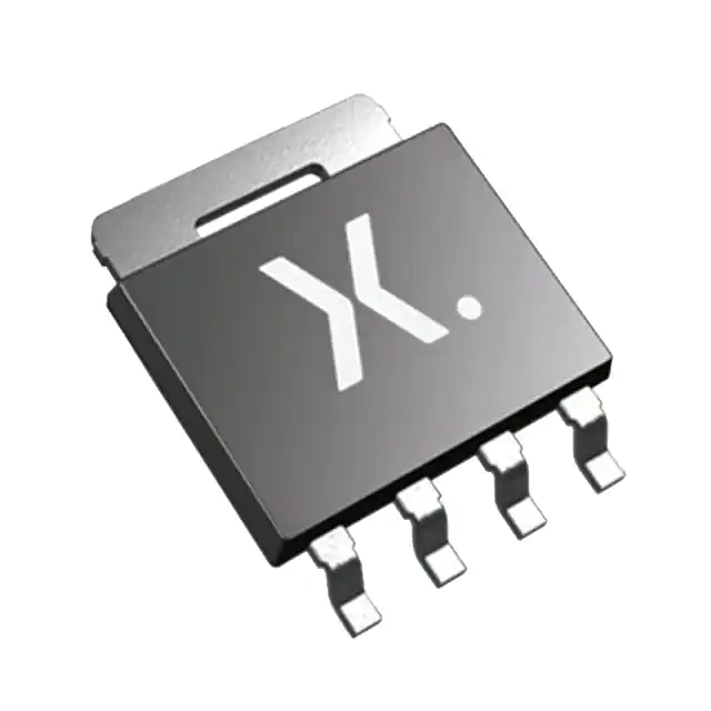
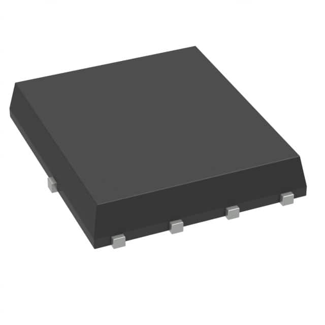
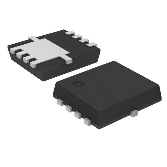
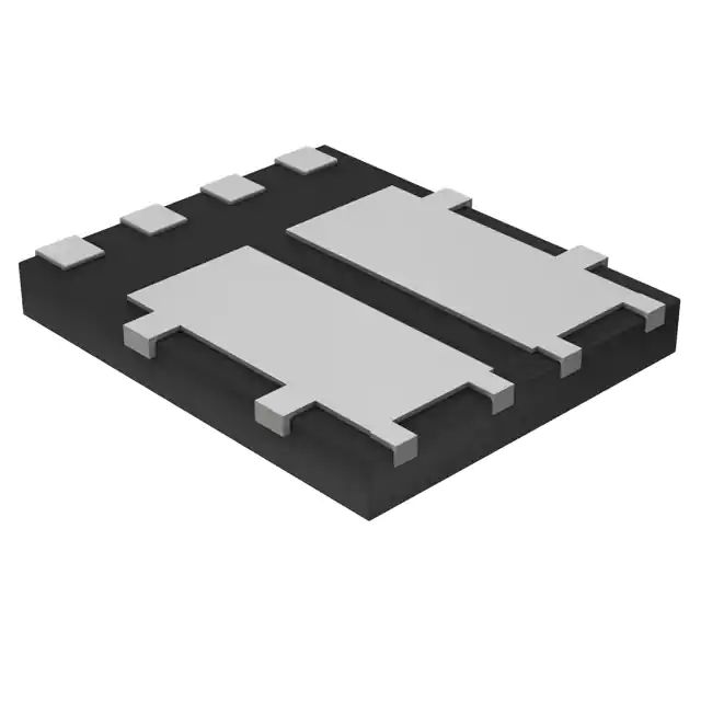
Package: PowerPAK® SO-8L (PPKSO8LWLA), 5.0 mm × 6.15 mm footprint with exposed drain thermal pad on bottom side; compliant with JEDEC MO-229 and RoHS/REACH.

Pin/Terminal Circuit Role Design Meaning
1, 2, 3, 4 (S)SourceFour parallel source terminals reduce parasitic inductance and improve current sharing in high-di/dt applications
5 (G)GateSingle gate input with Rg = 0.8–2.4 Ω - supports controlled turn-on/turn-off without external gate resistor
6, 7, 8 (D)DrainThree drain terminals connected to internal die drain metallization and bottom thermal pad for low-inductance, high-current path

Key Features

Feature Design Value
AEC-Q101 qualifiedValidated for automotive use including temperature cycling, HTRB, and UHAST per Rev. A test plan
100 % Rg and UIS testedEvery unit screened for gate resistance consistency and unclamped inductive switching robustness
TrenchFET® Gen IV processOptimized cell pitch and trench depth yield 25 % lower RDS(on) vs. prior generation at same voltage class
Exposed drain thermal padBottom-side copper pad enables <1.7 °C/W junction-to-case thermal path when soldered to PCB copper pour
Low Qgd/Qg ratioQgd = 2 nC / Qg ≈ 10 % - minimizes Miller effect and improves hard-switching stability

Applications

Engine Control Unit (ECU) Fuel Injector Driver Automotive HVAC Blower Motor Controller

Use Scenario: High-speed switching of 12 V fuel injectors with peak currents up to 60 A and 1 ms pulse widths.

IC Role / Device Role / Timing Role: High-side N-channel switch controlling injector coil energization/de-energization with integrated body diode freewheeling.

Use Value: 9.7 mΩ RDS(on) limits conduction loss to <0.36 W at 60 A, while 24 mJ EAS withstands inductive kickback without snubber.

Use Scenario: PWM-controlled 24 V blower motor in cabin air handling units requiring >50 A continuous current.

IC Role / Device Role / Timing Role: Low-side switching element in half-bridge topology, leveraging low Qg for 20 kHz PWM efficiency.

Use Value: 19–29 nC total gate charge reduces driver power dissipation; 175 °C TJ rating sustains operation near hot engine bay components.

12 V/48 V Mild Hybrid DC-DC Converter Automotive LED Headlamp Matrix Driver

Use Scenario: Synchronous rectifier in bidirectional buck-boost converter interfacing 12 V starter battery and 48 V Li-ion auxiliary bus.

IC Role / Device Role / Timing Role: High-efficiency synchronous FET with fast body diode recovery (trr = 27–54 ns) minimizing reverse recovery loss.

Use Value: Qrr = 20–40 nC and low Coss (621–870 pF) reduce switching losses during zero-voltage transition (ZVT) operation.

Use Scenario: Individual channel switch for adaptive LED headlamps with dynamic beam shaping, requiring precise current control and thermal resilience.

IC Role / Device Role / Timing Role: High-side current sink enabling PWM dimming at >1 kHz with minimal thermal derating.

Use Value: RthJC = 1.68 °C/W allows direct thermal coupling to metal-core PCB, maintaining <125 °C junction temp at 5 A LED load.

Equivalent & Alternatives

The following parts are listed as comparable options for similar N-channel 60 V automotive MOSFET applications.

Alternative Part Technical Difference Application Difference Selection Advice
STL220N6F7RDS(on) = 1.2 mΩ higher at 10 V; Qg = 32 nC (66 % higher); AEC-Q101 qualifiedHigher conduction loss limits max continuous current to 60 A at same TC; less suitable for high-frequency ZVS convertersPrefer SQJ166ELP-T1_GE3 where gate drive strength is limited or switching frequency exceeds 250 kHz
IRF1660SC2TO-263 package; RDS(on) = 10.5 mΩ; no AEC-Q101 qualification; RthJC = 1.5 °C/WLarger footprint and non-automotive qualification restrict use to industrial or commercial power suppliesChoose SQJ166ELP-T1_GE3 for space-constrained automotive PCBs requiring certified reliability and SO-8L compatibility

Compared with STL220N6F7 and IRF1660SC2, SQJ166ELP-T1_GE3 offers the lowest combined conduction/switching loss in compact PowerPAK® SO-8L, with full AEC-Q101 validation and optimized Qgd/Qg for stable high-frequency operation in safety-critical vehicle subsystems.

Availability

SQJ166ELP-T1_GE3 is available at Aetrix Electronics and suitable for automotive powertrain control, body electronics, and ADAS subsystems requiring stable component supply, long-term lifecycle support, and traceable sourcing.

Supply support for SQJ166ELP-T1_GE3 includes scheduled delivery planning, volume procurement assistance, BOM continuity management, traceable sourcing, and lifecycle availability coordination for OEM customers, industrial embedded developers, connected-device designers, and electronics production programs.

Manufacturer

Vishay Siliconix designs and manufactures discrete semiconductors, specializing in power MOSFETs, diodes, and optoelectronics with emphasis on ruggedness, precision, and automotive qualification.

The SQJ166ELP-T1_GE3 belongs to Vishay's TrenchFET® Gen IV automotive MOSFET family, engineered specifically for high-current, high-temperature switching in engine management, transmission control, and electrified chassis systems.

FAQ

What is the maximum junction temperature rating for SQJ166ELP-T1_GE3?

The SQJ166ELP-T1_GE3 has a specified operating junction temperature range of -55 °C to +175 °C, validated per AEC-Q101 stress testing including HTGB and temperature cycling. This rating enables deployment in under-hood environments such as engine control modules and transmission valve body controllers where ambient temperatures exceed 125 °C.

Does SQJ166ELP-T1_GE3 support logic-level gate drive?

Yes, SQJ166ELP-T1_GE3 delivers RDS(on) = 15.0 mΩ at VGS = 4.5 V, making it compatible with standard 5 V and 3.3 V microcontroller outputs without requiring gate boost circuitry. Its gate threshold voltage range of 1.5–2.5 V ensures reliable turn-on across process and temperature variation.

Is SQJ166ELP-T1_GE3 qualified for automotive applications?

Yes, SQJ166ELP-T1_GE3 is fully AEC-Q101 qualified per Rev. A test plan, including 100 % Rg and UIS screening, HTRB, and temperature cycling. It carries Vishay's automotive material categorization per Doc. #99912 and is approved for use in safety-critical powertrain and body control modules.

How is thermal performance validated for SQJ166ELP-T1_GE3?

Thermal resistance values for SQJ166ELP-T1_GE3 - RthJC = 1.68 °C/W and RthJA = 42 °C/W - are measured per JESD51-14 on a 1" × 1" FR4 PCB with 2 oz. copper. The exposed drain pad must be soldered to a minimum 100 mm² copper pour to achieve published RthJC; land pattern follows Vishay Doc. #78020.

What is the body diode reverse recovery performance of SQJ166ELP-T1_GE3?

The SQJ166ELP-T1_GE3 body diode exhibits trr = 27–54 ns and Qrr = 20–40 nC at IF = 10 A and di/dt = 100 A/μs. These values enable efficient freewheeling in synchronous rectification and inductive load switching, reducing voltage overshoot and EMI compared to standard silicon diodes.

SQJ166ELP-T1_GE3 Specifications

Product attributes
Attribute value
Manufacturer:
Vishay Siliconix
Series:
TrenchFET® Gen IV
Package/Case:
PowerPAK® SO-8
Packaging:
Tape & Reel (TR)
Product Status:
Active
FET Type:
N-Channel
Technology:
MOSFET (Metal Oxide)
Drain to Source Voltage (Vdss):
60 V
Current - Continuous Drain (Id) @ 25°C:
67A (Tc)
Drive Voltage (Max Rds On, Min Rds On):
4.5V, 10V
Rds On (Max) @ Id, Vgs:
9.7mOhm @ 20A, 10V
Vgs(th) (Max) @ Id:
2.5V @ 250µA
Gate Charge (Qg) (Max) @ Vgs:
29 nC @ 10 V
Vgs (Max):
±20V
Input Capacitance (Ciss) (Max) @ Vds:
1903 pF @ 25 V
FET Feature:
-
Power Dissipation (Max):
89W (Tc)
Operating Temperature:
-55°C ~ 175°C (TJ)
Grade:
Automotive
Qualification:
AEC-Q101
Mounting Type:
Surface Mount
Supplier Device Package:
PowerPAK® SO-8

SQJ166ELP-T1_GE3 FAQ

1.How can I place an order for SQJ166ELP-T1_GE3 through Aetrix?

Please submit a Request for Quotation (RFQ) for SQJ166ELP-T1_GE3 on Aetrix. Our sales agent will provide a competitive quotation and guide you through the order confirmation once you accept the terms.

2.Are the price and stock information for SQJ166ELP-T1_GE3 reliable?

The price and inventory of SQJ166ELP-T1_GE3 are updated periodically and may fluctuate due to market conditions. Stock and pricing data are typically refreshed every 24 hours. Quotation validity for SQJ166ELP-T1_GE3 is usually 5 days.

3.What payment methods are accepted for SQJ166ELP-T1_GE3?

We accept Wire Transfer, PayPal, Credit Card, Western Union, MoneyGram, and Escrow for SQJ166ELP-T1_GE3 transactions.

Note: Certain payment methods may incur a processing fee.

4.How is shipping managed for SQJ166ELP-T1_GE3?

SQJ166ELP-T1_GE3 orders can be shipped via leading logistics carriers, including DHL, UPS, FedEx, TNT, or Registered Mail.

Once your SQJ166ELP-T1_GE3 order is processed, you will receive an email with the shipment details and tracking number.

Note: Tracking information may take up to 24 hours to appear. Express delivery typically takes 3–5 business days.

5.How can I obtain technical support or documentation for SQJ166ELP-T1_GE3?

For technical support, including SQJ166ELP-T1_GE3 datasheets, pinout diagrams, or application guidance, please contact our engineering support team. They can provide detailed documentation and assistance for your SQJ166ELP-T1_GE3 requirements.

6.How does Aetrix verify that SQJ166ELP-T1_GE3 is sourced from the original manufacturer or authorized distributors?

All SQJ166ELP-T1_GE3 products on Aetrix are procured from qualified distributors and authorized channels. Our dedicated quality assurance team conducts strict verification, including traceability checks and, if necessary, third-party testing. This ensures that SQJ166ELP-T1_GE3 meets industry standards.

7.What is the process for return or replacement of SQJ166ELP-T1_GE3?

All SQJ166ELP-T1_GE3 units undergo pre-shipment inspection (PSI). If there is an issue with SQJ166ELP-T1_GE3, returns or replacements are accepted under the following conditions:

1.Quantity discrepancies, incorrect items, or visible external defects (such as breakage or corrosion), acknowledged by Aetrix.

2.The issue is reported within 90 days of delivery.

3.The SQJ166ELP-T1_GE3 part is unused and in its original packaging.

Return procedure for SQJ166ELP-T1_GE3:

1.Submit a request within 90 days.

2.Obtain a Return Material Authorization (RMA) from Aetrix.

SQJ166ELP-T1_GE3 Tags
  • SQJ166ELP-T1_GE3
  • SQJ166ELP-T1_GE3 PDF
  • SQJ166ELP-T1_GE3 Datasheet
  • SQJ166ELP-T1_GE3 Specifications
  • SQJ166ELP-T1_GE3 Images
  • Vishay Siliconix
  • Vishay Siliconix SQJ166ELP-T1_GE3
  • Buy SQJ166ELP-T1_GE3
  • SQJ166ELP-T1_GE3 Price
  • SQJ166ELP-T1_GE3 Distributor
  • SQJ166ELP-T1_GE3 Supplier
  • SQJ166ELP-T1_GE3 Wholesale
Related Products
BSZ180P03NS3EGATMA1
BSZ180P03NS3EGATMA1

Infineon Technologies
SIRA14DP-T1-GE3
SIRA14DP-T1-GE3

Vishay Siliconix

AO4419
AO4419

Alpha & Omega Semiconductor Inc.
SISA14BDN-T1-GE3
SISA14BDN-T1-GE3

Vishay Siliconix

PSMN9R5-30YLC,115
PSMN9R5-30YLC,115

Nexperia USA Inc.

BUK9Y21-40E,115
BUK9Y21-40E,115

Nexperia USA Inc.

RTQ035N03HZGTR
RTQ035N03HZGTR

Rohm Semiconductor

FDMS7680
FDMS7680

onsemi

RQ3E180BNTB
RQ3E180BNTB

Rohm Semiconductor

STL6N2VH5
STL6N2VH5

STMicroelectronics

DMPH4029LFGQ-7
DMPH4029LFGQ-7

Diodes Incorporated

DMT6015LSS-13
DMT6015LSS-13

Diodes Incorporated

Tech Hub

Search

Search

PRODUCT

PRODUCT

PHONE

PHONE

USER

USER