
 My Inquiry
 My Account


Microchip Technology U3280M-NFBY-18
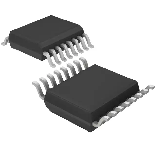
- Part No.:
- U3280M-NFBY-18
- Manufacturer:
- Microchip Technology
- Category:
- RFID, RF Access, Monitoring ICs
- Package:
- 16-LSSOP (0.154", 3.90mm Width)
- Datasheet:
-
 U3280M-NFBY-18.pdf
- Description:
- IC RFID TRANSP 100-150KHZ 16SSO
- Quantity:
- Payment:

- Shipping:

Inventory:2,520
Please send an inquiry. Send us your inquiry, and we will respond immediately.
Product details
Overview
U3280M-NFBY-18 from Microchip Technology (formerly Atmel) is a contactless transponder interface IC designed to power and communicate with low-power microcontrollers in passive RFID systems. It provides dual-mode power management (RF field or battery), 512-bit EEPROM, two-wire serial interface, and field clock extraction - enabling wireless sensor nodes and access control tags operating at 100–150 kHz with up to 10 kbaud data rate.
For engineers reviewing the U3280M-NFBY-18 datasheet, U3280M-NFBY-18 pinout, U3280M-NFBY-18 application, or U3280M-NFBY-18 equivalent, this device serves as a complete front-end for battery-assisted or fully passive 125 kHz transponders - supporting wake-up via NGAP, bi-phase/Manchester modulation control, and EEPROM-based configuration storage without external logic.
Technical Context
The U3280M-NFBY-18 integrates a rectifier, field clock extractor (FC), gap detector (NGAP), damping modulator (MOD), and automatic power management that switches between VBatt and coil-derived VDD. Its internal 512-bit EEPROM (32 × 16-bit) is accessed via SDA/SCL using I²C-compatible timing with acknowledge polling and auto-increment read modes.
It supports three operational states: field-only, battery-only, and hybrid - controlled via serial command (e.g., 11xx0111b disables automatic switching). The modulator accepts digital input on MOD to damp the LC tank, generating ~2 Vpp coil voltage stroke; NGAP delivers synchronized field/gap detection with <50 µs response time for microcontroller wake-up and demodulation.
Key Specifications
| Parameter | Value and Actual Design Meaning |
|---|---|
| Operating Frequency | 100–150 kHz - matches ISO/IEC 18000-2 and proprietary 125 kHz RFID base stations; requires parallel LC antenna tuned to this band. |
| Data Rate (R/O) | Up to 10 kbaud - enables fast tag identification and sensor telemetry in short-range industrial telemetry applications. |
| EEPROM Size | 512-bit (32 × 16-bit) - stores unique ID, calibration data, or configuration bits; supports 500k erase/write cycles and 10-year data retention at 25°C. |
| Power Supply Modes | Battery (VBatt: 2.0–6.5 V) + contactless field - automatic switchover with VFDon = 2.5 V (typ), VFDoff = 0.8 V; VDDC limited to 2.9 V during field supply. |
| Serial Interface | Two-wire (SCL/SDA), I²C-compatible - max 100 kHz clock, 0.2 ms power-up-to-read latency, and acknowledge polling for write completion. |
| Modulation Support | Bi-phase and Manchester encoding - enabled via serial control bytes (1100x111b / 1101x111b); MOD pin allows direct digital damping control. |
| Quiescent Current | 0.4 µA sleep current - extends battery life in always-on wireless sensors; field supply draws only 40–80 µA typical. |
Pinout & Package
U3280M-NFBY-18 is housed in a 16-pin SSOP (SSO16) package with 0.635 mm pitch, 7.0 mm × 5.0 mm body, and Pb-free finish. Pin 1 is marked by a dot; pins 3–6 and 11–14 are NC. Coil connections occupy pins 15 and 16; power and serial I/O are distributed across VDD, VBatt, SDA, SCL, NRST, VSS, FC, MOD, and NGAP.
| Pin/Terminal | Circuit Role | Design Meaning |
|---|---|---|
| VBatt (Pin 1) | Battery supply input | Accepts 2.0–6.5 V DC; powers device when field is absent; feeds internal regulator for VDD during battery mode. |
| VDD (Pin 2) | Main power output | Supplies microcontroller and EEPROM; requires 0.5–10 µF buffer capacitor to sustain operation during field gaps/damping. |
| SCL (Pin 3) | Serial clock input/output | Master-generated clock for EEPROM access; also used as modulator clock in Bi-phase/Manchester mode. |
| NRST (Pin 4) | Bi-directional reset | Input: triggers reset when pulled low; output: asserts reset pulse to MCU during field→battery switch. |
| SDA (Pin 5) | Serial data I/O | Bi-directional data line for EEPROM reads/writes; doubles as modulator data input in special serial modes. |
| VSS (Pin 6) | Ground reference | Common return for all analog and digital circuits; must be low-impedance connection to minimize noise coupling. |
| FC (Pin 8) | Field clock output | Provides extracted 100–150 kHz clock signal to MCU timer for synchronous modulation/demodulation. |
| MOD (Pin 9) | Modulation control input | Digital input controlling coil damping: MOD = 1 damps coil (lowers Vcoil), MOD = 0 releases damping (raises Vcoil). |
| NGAP (Pin 10) | Field/gap detection output | Active-high signal indicating presence of RF field; used for MCU wake-up interrupt and gap-based data reception. |
| Coil 1 (Pin 15) | Antenna resonant circuit input | Connects to one terminal of parallel LC tank; forms part of rectifier input stage for field energy harvesting. |
| Coil 2 (Pin 16) | Antenna resonant circuit input | Connects to second terminal of LC tank; differential input improves noise immunity and field coupling efficiency. |
Key Features
| Feature | Design Value |
|---|---|
| Automatic Power Management | Seamlessly switches between battery and field supply using VFDon/VFDoff thresholds; eliminates need for external power selectors or firmware supervision. |
| Integrated Field Clock Extractor | Delivers clean 100–150 kHz clock (FC pin) directly from the RF field - enables precise timing for synchronous demodulation without external crystal or PLL. |
| Gap Detection with Wake-up Output | NGAP pin asserts high within 1–50 µs of field application - provides deterministic, low-latency wake-up signal to MCU interrupt pin for ultra-low-power operation. |
| On-chip 512-bit EEPROM | Organized as 32 × 16-bit rows; accessible via standard two-wire protocol with auto-increment reads and acknowledge polling - reduces host MCU code footprint and external memory cost. |
| Configurable Modulation Engine | Supports both Bi-phase and Manchester encoding via serial command; MOD pin allows real-time digital control of damping - simplifies protocol adaptation across reader ecosystems. |
Applications
| Access Control Tags | Wireless Sensor Nodes |
|---|---|
|
Use Scenario: Passive or semi-passive RFID tags used in door locks, asset tracking, or secure entry systems where battery life and field reliability are critical. IC Role / Device Role / Timing Role: Transponder interface providing contactless power, wake-up via NGAP, and secure ID storage in on-chip EEPROM. Use Value: Eliminates need for separate power management IC and EEPROM; enables >10-year battery life in hybrid mode with field-assisted wake-up and data transmission. |
Use Scenario: Industrial condition monitoring sensors deployed in rotating machinery, HVAC ducts, or hazardous zones where wired connectivity is impractical. IC Role / Device Role / Timing Role: Front-end for microcontroller-based sensor acquisition - supplies power from reader field, extracts FC clock for timing-critical ADC sampling, and stores calibration data. Use Value: Enables zero-maintenance, battery-backed sensing with field-triggered data upload; 0.4 µA sleep current extends operational life beyond 5 years. |
| Contactless Position Sensors | Telemetry Beacons |
|
Use Scenario: Non-contact alignment verification in CNC tools, robotic arms, or medical equipment where metal interference prohibits optical or inductive proximity sensors. IC Role / Device Role / Timing Role: Transponder interface powering position-sensing MCU and transmitting encoded angular/linear position via field modulation. Use Value: Supports sub-millimeter resolution via Manchester-encoded position words stored in EEPROM; NGAP-driven wake-up ensures immediate response to reader interrogation. |
Use Scenario: Remote environmental monitoring beacons (temperature, humidity, pressure) deployed in utility meters, agricultural fields, or infrastructure assets. IC Role / Device Role / Timing Role: Low-power transponder managing intermittent field-powered data bursts, storing historical readings in EEPROM, and synchronizing transmission using FC clock. Use Value: Achieves >3 km read range in optimized 125 kHz systems; 500k EEPROM endurance supports daily logging for >13 years without wear-out. |
Equivalent & Alternatives
The following parts are listed as comparable options for similar transponder interface applications.
| Alternative Part | Technical Difference | Application Difference | Selection Advice |
|---|---|---|---|
| SLI52120 (Infineon) | Integrated 13.56 MHz HF frontend; no battery support; fixed 64-bit UID; no EEPROM; higher data rate (up to 106 kbit/s). | Designed for ISO 14443-A/B smart card readers - unsuitable for 125 kHz passive sensor or access control systems requiring battery backup. | Select only for HF (13.56 MHz) applications with no need for dual power mode or local nonvolatile storage. |
| TDA8029 (NXP) | 125 kHz transponder IC with integrated LDO and watchdog; no EEPROM; supports only ASK modulation; no FC/NGAP dedicated pins. | Lacks field clock extraction and gap-detect outputs - requires external timing recovery and interrupt generation for wake-up functionality. | Choose when system-level timing is handled externally and EEPROM is provided by host MCU; not drop-in for U3280M-NFBY-18 designs. |
Compared with SLI52120 and TDA8029, the U3280M-NFBY-18 uniquely combines 125 kHz operation, battery+field dual supply, on-chip EEPROM, dedicated FC/NGAP timing signals, and software-controllable modulation - making it the only option among the three for self-contained, long-life, field-wakeable transponder nodes.
Availability
U3280M-NFBY-18 is available at Aetrix Electronics and suitable for access control systems, wireless sensor networks, and telemetry beacons requiring stable component supply, long-term lifecycle support, and RoHS-compliant packaging.
Supply support for U3280M-NFBY-18 includes scheduled delivery planning, volume procurement assistance, BOM continuity management, traceable sourcing, and lifecycle availability coordination for OEM customers, industrial embedded developers, connected-device designers, and electronics production programs.
Manufacturer
Microchip Technology acquired Atmel in 2016 and maintains its legacy RFID product lines. The company specializes in microcontrollers, analog, and security ICs for industrial, automotive, and IoT applications.
The U3280M-NFBY-18 belongs to Atmel's transponder interface product line, engineered specifically for battery-assisted and fully passive 125 kHz RFID systems - emphasizing ultra-low power, field synchronization, and embedded nonvolatile configuration storage.
FAQ
What is the primary function of the U3280M-NFBY-18 in an RFID system?
The U3280M-NFBY-18 serves as a transponder interface IC that powers and communicates with a microcontroller using contactless RF energy. It rectifies magnetic field energy from a 100–150 kHz reader, manages seamless switching between battery and field supply, provides field clock (FC) and gap detection (NGAP) signals, and hosts 512-bit EEPROM for persistent data storage - all within a single SSOP-16 package. The U3280M-NFBY-18 enables fully autonomous, low-power tag operation without external power management or timing components.
Can the U3280M-NFBY-18 operate without a battery?
Yes, the U3280M-NFBY-18 can operate in fully passive mode using only RF field energy harvested through its Coil 1 and Coil 2 pins. Its internal rectifier and regulator generate VDD from the LC-resonant circuit, powering both the U3280M-NFBY-18 and an attached microcontroller. However, battery (VBatt) is required for operation when the field is absent - such as during deep sleep or offline sensor logging - and enables hybrid operation where the field wakes the system and battery sustains background tasks.
How does the NGAP pin function in U3280M-NFBY-18 wake-up applications?
The NGAP pin on the U3280M-NFBY-18 outputs a high-level signal (NGAP = 1) within 1–50 µs of RF field detection, serving as a hardware wake-up interrupt for the connected microcontroller. This eliminates polling and reduces average current consumption. When the field disappears, NGAP goes low, signaling end-of-interrogation. In battery-only mode, NGAP remains low unless field is present - ensuring deterministic, low-latency activation only when needed. The U3280M-NFBY-18 uses this signal internally to trigger power management state transitions.
What EEPROM access methods does the U3280M-NFBY-18 support?
The U3280M-NFBY-18 supports byte-wise, word-wise (16-bit), and sequential read/write operations via its two-wire serial interface. It uses a 5-bit row address (32 rows) with mode control bits to select high-byte-first or low-byte-first access and auto-increment/decrement addressing. Write cycles require acknowledge polling due to 9–12 ms internal erase-write latency; read operations have 0.2 ms power-up-to-access time. All EEPROM functions - including initialization after reset - are implemented through defined control bytes (e.g., 11xx0111b for power management control), and the U3280M-NFBY-18 enforces strict timing per I²C-compatible protocol.
Is the U3280M-NFBY-18 pin-compatible with other Atmel transponder interfaces?
No, the U3280M-NFBY-18 has a unique 16-pin SSOP footprint and pin assignment optimized for its dual-coil, dual-power architecture. While earlier Atmel transponder ICs like the U2270B share functional similarities (e.g., 125 kHz operation, modulation), they use different packages (e.g., SOIC-8), lack EEPROM, omit FC/NGAP dedicated pins, and do not support battery-field automatic switchover. Migration to or from the U3280M-NFBY-18 requires PCB layout revision, firmware adaptation for serial command set, and antenna tuning adjustments - confirming the U3280M-NFBY-18 as a standalone solution rather than a drop-in upgrade.
U3280M-NFBY-18 Specifications
- Product attributes
- Attribute value
- Manufacturer:
- Microchip Technology
- Series:
- U3280M
- Package/Case:
- 16-LSSOP (0.154", 3.90mm Width)
- Packaging:
- Tape & Reel (TR)
- Product Status:
- Obsolete
- Type:
- RFID Transponder
- Frequency:
- 100kHz ~ 150kHz
- Standards:
- -
- Interface:
- -
- Voltage - Supply:
- 2V ~ 6.5V
- Operating Temperature:
- -40°C ~ 85°C
- Grade:
- -
- Qualification:
- -
- Mounting Type:
- Surface Mount
- Supplier Device Package:
- 16-SSO
U3280M-NFBY-18 FAQ
1.How can I place an order for U3280M-NFBY-18 through Aetrix?
Please submit a Request for Quotation (RFQ) for U3280M-NFBY-18 on Aetrix. Our sales agent will provide a competitive quotation and guide you through the order confirmation once you accept the terms.
2.Are the price and stock information for U3280M-NFBY-18 reliable?
The price and inventory of U3280M-NFBY-18 are updated periodically and may fluctuate due to market conditions. Stock and pricing data are typically refreshed every 24 hours. Quotation validity for U3280M-NFBY-18 is usually 5 days.
3.What payment methods are accepted for U3280M-NFBY-18?
We accept Wire Transfer, PayPal, Credit Card, Western Union, MoneyGram, and Escrow for U3280M-NFBY-18 transactions.
Note: Certain payment methods may incur a processing fee.
4.How is shipping managed for U3280M-NFBY-18?
U3280M-NFBY-18 orders can be shipped via leading logistics carriers, including DHL, UPS, FedEx, TNT, or Registered Mail.
Once your U3280M-NFBY-18 order is processed, you will receive an email with the shipment details and tracking number.
Note: Tracking information may take up to 24 hours to appear. Express delivery typically takes 3–5 business days.
5.How can I obtain technical support or documentation for U3280M-NFBY-18?
For technical support, including U3280M-NFBY-18 datasheets, pinout diagrams, or application guidance, please contact our engineering support team. They can provide detailed documentation and assistance for your U3280M-NFBY-18 requirements.
6.How does Aetrix verify that U3280M-NFBY-18 is sourced from the original manufacturer or authorized distributors?
All U3280M-NFBY-18 products on Aetrix are procured from qualified distributors and authorized channels. Our dedicated quality assurance team conducts strict verification, including traceability checks and, if necessary, third-party testing. This ensures that U3280M-NFBY-18 meets industry standards.
7.What is the process for return or replacement of U3280M-NFBY-18?
All U3280M-NFBY-18 units undergo pre-shipment inspection (PSI). If there is an issue with U3280M-NFBY-18, returns or replacements are accepted under the following conditions:
1.Quantity discrepancies, incorrect items, or visible external defects (such as breakage or corrosion), acknowledged by Aetrix.
2.The issue is reported within 90 days of delivery.
3.The U3280M-NFBY-18 part is unused and in its original packaging.
Return procedure for U3280M-NFBY-18:
1.Submit a request within 90 days.
2.Obtain a Return Material Authorization (RMA) from Aetrix.
U3280M-NFBY-18 Tags

-
SL2S2602FTBX
NXP Semiconductors

-
ST25DV04K-IER6S3
STMicroelectronics

-
ST25DV04K-IER6C3
STMicroelectronics
-
LXMSJZNCMD-217
Murata Electronics

-
NT3H2111W0FTTJ
NXP Semiconductors

-
NT3H2111W0FHKH
NXP Semiconductors

-
M24LR04E-RMC6T/2
STMicroelectronics
-
ST25DV04KC-JF6D3
STMicroelectronics

-
ST25DV64KC-IE6S3
STMicroelectronics

-
ST25DV64K-IER6T3
STMicroelectronics
-
NT3H2211W0FTTJ
NXP Semiconductors
-
NT3H2211W0FHKH
NXP Semiconductors
Tech Hub

TTL and CMOS logic families differ in thresholds, loading, output drive, power and timing. This engineering guide compares 74HC and 74HCT, calculates noise margins and checks 3.3 V/5 V compatibility.

A practical engineering guide to 3.3V and 5V logic compatibility, input thresholds, resistor dividers, translator ICs, MOSFET level shifting, I2C pull-ups, timing limits and power-sequencing risks.

The 74HC595 uses push-pull logic outputs, while the TPIC6B595 uses 50 V open-drain DMOS sinks for higher-power loads. This guide compares timing, current limits, 3.3 V interfacing, load wiring, thermal…

The 74HC595 converts serial data into eight stable parallel outputs. This guide covers pin functions, shift and storage timing, OE and MR behavior, drive-current limits, cascading, voltage compatibilit…

A technical comparison of level-sensitive latches and edge-triggered flip-flops, covering timing windows, setup and hold limits, master–slave operation, time borrowing, race-through, HDL inference and…

A D latch stores one bit while Enable controls when data can pass. This reference covers gate-level operation, truth tables, transparency, setup and hold timing, LE versus OE, common ICs and practical …

An SR latch stores one bit through cross-coupled feedback. This engineering reference covers NOR and NAND implementations, truth tables, forbidden-state recovery, gated operation, switch debouncing, fa…

Latch circuits retain one bit through feedback. This technical reference covers SR and D latches, truth tables, transparency, timing limits, latch-versus-flip-flop behavior, applications and common log…

An engineering guide to LED driver operation, constant-current and constant-voltage outputs, linear and switching topologies, dimming, IC selection, calculations, replacement compatibility, and fault c…

Operational amplifier guide covering op amp basics, feedback, ideal vs real op amps, common configurations, buffer circuits, offset, bias current, gain-bandwidth, slew rate, rail-to-rail limits and sel…


