
 My Inquiry
 My Account


Diodes Incorporated DMN2029UVT-7
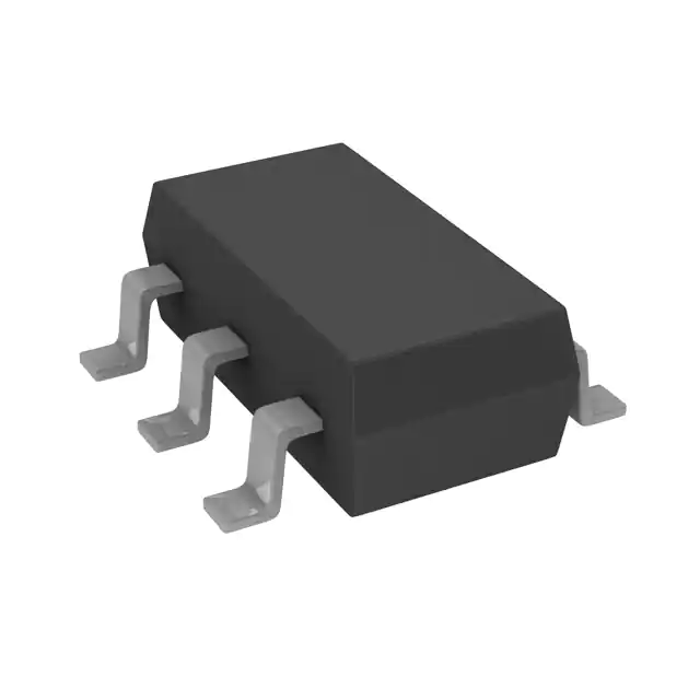
- Part No.:
- DMN2029UVT-7
- Manufacturer:
- Diodes Incorporated
- Category:
- FETs, MOSFETs
- Package:
- SOT-23-6 Thin, TSOT-23-6
- Datasheet:
-
 DMN2029UVT-7.pdf
- Description:
- MOSFET N-CH 6.8A TSOT26
- Quantity:
- Payment:

- Shipping:

Inventory:4,512
Please send an inquiry. Send us your inquiry, and we will respond immediately.
Product details
Overview
DMN2029UVT from Diodes Incorporated is an N-channel enhancement-mode MOSFET in TSOT26 package, rated for 20V VDSS, 24 mΩ RDS(ON) at VGS = 4.5V, and 6.8A continuous drain current at TA = +25°C. It delivers low on-resistance and fast switching for high-efficiency DC-DC converters and power management functions in space-constrained portable electronics.
For engineers reviewing the DMN2029UVT datasheet, DMN2029UVT pinout, DMN2029UVT application, or DMN2029UVT equivalent, key selection criteria include its 2.5V logic-level gate drive capability, 7.1 nC total gate charge, 646 pF input capacitance, and thermal resistance of 74 °C/W under enhanced PCB layout - all critical for compact, thermally managed buck regulators and LED backlight drivers.
Technical Context
This MOSFET employs a trench-gate silicon process optimized for low RDS(ON) while maintaining controlled gate charge (Qg = 7.1 nC) and fast switching (tr = 139 ns, tf = 433 ns). Its gate threshold voltage range (0.4–1.5 V) ensures reliable turn-on with 2.5V–4.5V microcontroller I/O.
The device integrates a body diode with VSD = 0.65–1.2 V at IS = 1.3 A and exhibits low reverse recovery charge (QRR = 148 nC), supporting synchronous rectification and flyback topologies without external Schottky supplementation.
Key Specifications
| Parameter | Value and Actual Design Meaning |
|---|---|
| VDSS | 20 V - Supports input rails up to 18 V in 3.3 V/5 V system power stages. |
| RDS(ON) | 24 mΩ @ VGS = 4.5V - Enables ≤150 mW conduction loss at 6.2 A in compact DC-DC output switches. |
| ID (max) | 6.8 A @ TA = +25°C - Sustains peak load currents in single-phase POL converters with 2 oz copper and thermal vias. |
| Qg | 7.1 nC - Reduces gate driver power demand and enables >1 MHz switching with low-side gate resistors ≤6 Ω. |
| Ciss | 646 pF - Limits Miller-induced shoot-through risk in half-bridge configurations with moderate dV/dt. |
| TJ range | −55 to +150 °C - Qualified for industrial and extended-temperature embedded power modules. |
Pinout & Package
Package: TSOT26 - 6-pin ultra-thin surface-mount package (2.9 × 1.6 × 0.6 mm), molded plastic with UL 94V-0 rating, tin-finished copper leadframe, moisture sensitivity level 1.
| Pin/Terminal | Circuit Role | Design Meaning |
|---|---|---|
| 1 (S) | Source | Common return path for drain current; tied to ground or low-side reference in buck/synchronous rectifier topologies. |
| 2 (G) | Gate | Control terminal requiring <1.5 V threshold; driven directly by 2.5 V GPIO or dedicated gate driver IC. |
| 3 (D) | Drain | High-side switching node; connects to input rail or inductor in step-down converters. |
| 4 (D) | Drain | Internally paralleled with Pin 3 to reduce package inductance and improve current sharing in high-frequency operation. |
| 5 (D) | Drain | Third drain connection enhancing thermal and electrical performance; used for PCB copper pour attachment in thermal pads. |
| 6 (S) | Source | Second source terminal providing low-inductance return path; connected to ground plane via multiple vias for EMI reduction. |
Key Features
| Feature | Design Value |
|---|---|
| Logic-level gate drive | Operates fully enhanced at VGS ≥ 2.5 V - eliminates need for level-shifting circuitry in 3.3 V MCU-controlled power stages. |
| Low RDS(ON) × Qg figure-of-merit | 24 mΩ × 7.1 nC = 170 mΩ·nC - balances conduction and switching losses for optimal efficiency at 500 kHz–2 MHz. |
| Enhanced thermal dissipation | RθJA = 74 °C/W with 2 oz copper + thermal vias - supports 1.7 W steady-state power in minimal board area. |
| Green, RoHS-compliant construction | Halogen- and antimony-free molding compound (<900 ppm Br/Cl, <1000 ppm Sb) - meets IPC-1752A environmental reporting requirements. |
Applications
| DC-DC Buck Converter | LED Backlight Driver |
|---|---|
Use Scenario: Step-down regulation from 12 V to 5 V/3.3 V in portable medical monitors and handheld test equipment. IC Role / Device Role: Low-side synchronous rectifier switch in integrated buck controller designs. Use Value: 24 mΩ RDS(ON) reduces conduction loss by 35% vs. comparable 30 mΩ MOSFETs, extending battery runtime by >8% at 4 A load. | Use Scenario: Constant-current dimming control for edge-lit LCD panels in automotive infotainment displays. IC Role / Device Role: PWM-controlled current sink for white LED strings operating at 20–30 mA per channel. Use Value: Fast 139 ns rise time enables precise 100–1000 Hz PWM dimming without visible flicker or current overshoot. |
| Power Management Unit (PMU) | Load Switch for USB Peripherals |
Use Scenario: Independent power rail enable/disable in multi-rail FPGA or SoC carrier boards. IC Role / Device Role: High-efficiency load switch with controlled inrush limiting via gate resistor tuning. Use Value: 0.4–1.5 V VGS(TH) ensures clean turn-on at 1.8 V logic levels, eliminating false triggering during brown-out conditions. | Use Scenario: Hot-swap protection and sequencing for USB-C peripheral ports in docking stations. IC Role / Device Role: Reverse-current blocking switch between VBUS and downstream 5 V rail. Use Value: Body diode forward voltage ≤1.2 V at 1.3 A allows bidirectional conduction during plug insertion while minimizing voltage drop. |
Equivalent & Alternatives
The following parts are listed as comparable options for similar N-channel logic-level MOSFET applications.
| Alternative Part | Technical Difference | Application Difference | Selection Advice |
|---|---|---|---|
| DMN2029LVT-7 | Same die, but in SOT-26 (non-TSOT) package; RθJA = 109 °C/W (no thermal vias support); 0.7 W PD. | Limited to lower-power applications (<2.5 A continuous) due to higher thermal resistance and no exposed drain pad. | Select when board space permits larger footprint and thermal performance is secondary to cost. |
| AO3400A | 26 mΩ @ VGS = 4.5V, Qg = 12 nC, Ciss = 880 pF - higher switching loss and slower turn-off (td(off) = 14.5 ns vs. 1023 ns). | Less suitable for >1 MHz operation; requires stronger gate drive to achieve same efficiency. | Choose only if legacy qualification or second-source validation mandates AO34xx family compatibility. |
Compared with DMN2029LVT-7, the DMN2029UVT delivers 32% lower thermal resistance and 2.4× higher power handling; versus AO3400A, it achieves 41% lower Qg and 27% lower Ciss, enabling cleaner switching waveforms and reduced gate driver stress in high-frequency POL designs.
Availability
DMN2029UVT is available at Aetrix Electronics and suitable for DC-DC converters, LED backlight drivers, and load-switching applications requiring stable component supply, consistent parametric performance, and long-term production continuity.
Supply support for DMN2029UVT includes scheduled delivery planning, volume procurement assistance, BOM continuity management, traceable sourcing, and lifecycle availability coordination for OEM customers, industrial embedded developers, connected-device designers, and electronics production programs.
Manufacturer
Diodes Incorporated is a global manufacturer of discrete semiconductors and analog ICs, headquartered in Plano, Texas, with design, manufacturing, and sales operations across Asia, Europe, and North America.
The DMN2029UVT belongs to Diodes' "Ultra-Low RDS(ON) Logic-Level MOSFET" product line, engineered specifically for high-density, high-efficiency power conversion in portable, automotive, and industrial systems where thermal headroom and gate drive simplicity are critical.
FAQ
What is the maximum continuous drain current at 70°C ambient?
The DMN2029UVT supports 5.5 A continuous drain current at TA = +70°C with standard FR-4 PCB layout (2 oz copper, thermal vias). This derating reflects its 74 °C/W thermal resistance and 150 °C maximum junction temperature, ensuring safe operation in enclosed enclosures without forced airflow.
Does this MOSFET require a gate resistor for stability?
Yes - a 2–6 Ω series gate resistor is recommended to dampen ringing caused by gate-drain capacitance (Crss = 38 pF) and PCB trace inductance. Without it, fast edges may induce oscillation during turn-on/turn-off, increasing EMI and dynamic losses in high-frequency switching applications.
Can DMN2029UVT be used in reverse-biased configurations?
No - the device is not rated for reverse-biased operation (VDS < 0). Its body diode conducts only from source to drain (anode at S, cathode at D). For reverse-blocking or bidirectional current control, a complementary P-channel MOSFET or external diode must be added in series.
Is the TSOT26 package compatible with standard SMT reflow profiles?
Yes - the TSOT26 package is qualified for JEDEC J-STD-020 Level 1 moisture sensitivity and withstands peak reflow temperatures up to 260°C. Its tin-finished leadframe ensures reliable solder wetting using standard SnPb or lead-free SAC305 profiles, provided preheat and soak zones comply with Diodes' recommended ramp rates.
DMN2029UVT-7 Specifications
- Product attributes
- Attribute value
- Manufacturer:
- Diodes Incorporated
- Series:
- -
- Package/Case:
- SOT-23-6 Thin, TSOT-23-6
- Packaging:
- Tape & Reel (TR)
- Product Status:
- Active
- FET Type:
- N-Channel
- Technology:
- MOSFET (Metal Oxide)
- Drain to Source Voltage (Vdss):
- 20 V
- Current - Continuous Drain (Id) @ 25°C:
- 6.8A (Ta)
- Drive Voltage (Max Rds On, Min Rds On):
- 2.5V, 4.5V
- Rds On (Max) @ Id, Vgs:
- 24mOhm @ 6.2A, 4.5V
- Vgs(th) (Max) @ Id:
- 1.5V @ 250µA
- Gate Charge (Qg) (Max) @ Vgs:
- 7.1 nC @ 4.5 V
- Vgs (Max):
- ±10V
- Input Capacitance (Ciss) (Max) @ Vds:
- 646 pF @ 10 V
- FET Feature:
- -
- Power Dissipation (Max):
- 700mW (Ta)
- Operating Temperature:
- -55°C ~ 150°C (TJ)
- Grade:
- -
- Qualification:
- -
- Mounting Type:
- Surface Mount
- Supplier Device Package:
- TSOT-26
DMN2029UVT-7 FAQ
1.How can I place an order for DMN2029UVT-7 through Aetrix?
Please submit a Request for Quotation (RFQ) for DMN2029UVT-7 on Aetrix. Our sales agent will provide a competitive quotation and guide you through the order confirmation once you accept the terms.
2.Are the price and stock information for DMN2029UVT-7 reliable?
The price and inventory of DMN2029UVT-7 are updated periodically and may fluctuate due to market conditions. Stock and pricing data are typically refreshed every 24 hours. Quotation validity for DMN2029UVT-7 is usually 5 days.
3.What payment methods are accepted for DMN2029UVT-7?
We accept Wire Transfer, PayPal, Credit Card, Western Union, MoneyGram, and Escrow for DMN2029UVT-7 transactions.
Note: Certain payment methods may incur a processing fee.
4.How is shipping managed for DMN2029UVT-7?
DMN2029UVT-7 orders can be shipped via leading logistics carriers, including DHL, UPS, FedEx, TNT, or Registered Mail.
Once your DMN2029UVT-7 order is processed, you will receive an email with the shipment details and tracking number.
Note: Tracking information may take up to 24 hours to appear. Express delivery typically takes 3–5 business days.
5.How can I obtain technical support or documentation for DMN2029UVT-7?
For technical support, including DMN2029UVT-7 datasheets, pinout diagrams, or application guidance, please contact our engineering support team. They can provide detailed documentation and assistance for your DMN2029UVT-7 requirements.
6.How does Aetrix verify that DMN2029UVT-7 is sourced from the original manufacturer or authorized distributors?
All DMN2029UVT-7 products on Aetrix are procured from qualified distributors and authorized channels. Our dedicated quality assurance team conducts strict verification, including traceability checks and, if necessary, third-party testing. This ensures that DMN2029UVT-7 meets industry standards.
7.What is the process for return or replacement of DMN2029UVT-7?
All DMN2029UVT-7 units undergo pre-shipment inspection (PSI). If there is an issue with DMN2029UVT-7, returns or replacements are accepted under the following conditions:
1.Quantity discrepancies, incorrect items, or visible external defects (such as breakage or corrosion), acknowledged by Aetrix.
2.The issue is reported within 90 days of delivery.
3.The DMN2029UVT-7 part is unused and in its original packaging.
Return procedure for DMN2029UVT-7:
1.Submit a request within 90 days.
2.Obtain a Return Material Authorization (RMA) from Aetrix.
DMN2029UVT-7 Tags
-
BSZ180P03NS3EGATMA1
Infineon Technologies
-
SIRA14DP-T1-GE3
Vishay Siliconix

-
AO4419
Alpha & Omega Semiconductor Inc.
-
SISA14BDN-T1-GE3
Vishay Siliconix
-
PSMN9R5-30YLC,115
Nexperia USA Inc.
-
BUK9Y21-40E,115
Nexperia USA Inc.
-
RTQ035N03HZGTR
Rohm Semiconductor
-
FDMS7680
onsemi
-
RQ3E180BNTB
Rohm Semiconductor
-
STL6N2VH5
STMicroelectronics
-
DMPH4029LFGQ-7
Diodes Incorporated
-
DMT6015LSS-13
Diodes Incorporated
Tech Hub

An engineering guide to LED driver operation, constant-current and constant-voltage outputs, linear and switching topologies, dimming, IC selection, calculations, replacement compatibility, and fault c…

Operational amplifier guide covering op amp basics, feedback, ideal vs real op amps, common configurations, buffer circuits, offset, bias current, gain-bandwidth, slew rate, rail-to-rail limits and sel…

Jumper cables guide covering safe connection order, red and black clamp placement, final ground connection, cable gauge, length, clamp quality, copper vs CCA cables, jump starter comparison and battery…

LDO regulator guide covering low dropout voltage, power dissipation, thermal design, PSRR, output noise, capacitor stability, adjustable LDO circuits, LDO vs buck converter and datasheet selection chec…

Conditional Access Module guide covering CAM meaning, CI/CI+ interface, smart card authorization, DVB security workflow, TV and set-top box compatibility, internal electronics, ESD protection, connecto…

Guide to electronic component obsolescence covering EOL risk, PCN/PDN notices, last-time buy planning, replacement options, form-fit-function validation, counterfeit risk and BOM lifecycle management.

18650 battery guide covering lithium-ion cell basics, 3.6V/3.7V voltage, 4.2V charging, mAh and Wh capacity, protected cells, chargers, BMS, series-parallel packs, holders, welding and sourcing checks.…

Hall effect sensor guide covering working principle, linear and digital sensors, Arduino circuits, current sensing, speed detection, automotive applications, A3144 examples, signal filtering and datash…

Product Change Notification guide for electronic components, covering PCN meaning, PCN vs PDN/EOL, common change types, risk levels, form-fit-function review, engineering validation, BOM control, LTB/L…

A practical guide to blend door actuators, covering HVAC function, symptoms, location, AC and heater issues, reset and calibration, replacement cost, electrical diagnosis, compatibility checks, and rep…


