
 My Inquiry
 My Account


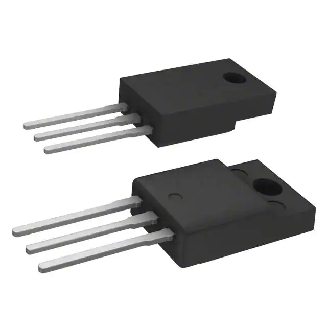
Renesas RJK5014DPP-E0#T2
- Part No.:
- RJK5014DPP-E0#T2
- Manufacturer:
- Renesas
- Category:
- FETs, MOSFETs
- Package:
- TO-220-3 Full Pack
- Datasheet:
-
 RJK5014DPP-E0#T2.pdf
- Description:
- RJK5014DPP-E0#T2 - SILICON N CHA
- Quantity:
- Payment:

- Shipping:

Inventory:12,236
Please send an inquiry. Send us your inquiry, and we will respond immediately.
Product details
Overview
RJK5014DPP-E0#T2 from Renesas Electronics is a silicon N-channel power MOSFET designed for high-speed switching in offline AC-DC power supplies and motor drive inverters, featuring 500 V VDSS, 0.325 Ω RDS(on) at 10 V VGS, and 19 A continuous drain current at Tc = 25 °C - deployed in industrial SMPS front-end switches and DC bus protection circuits.
For engineers reviewing the RJK5014DPP-E0#T2 datasheet, RJK5014DPP-E0#T2 pinout, RJK5014DPP-E0#T2 application, or RJK5014DPP-E0#T2 equivalent, this page delivers verified package mapping (TO-220FN), validated thermal impedance (3.57 °C/W), confirmed diode recovery time (320 ns), and real-world selection guidance against comparable 500 V MOSFETs with matching safe operating area limits.
Technical Context
This device implements a planar vertical DMOS structure optimized for rugged avalanche operation and low gate charge (Qg = 46 nC), enabling efficient hard-switching up to 100 kHz in flyback and forward converters. Its body diode exhibits 0.91 V forward voltage at 19 A and 320 ns reverse recovery time under 100 A/μs di/dt - critical for minimizing commutation losses in half-bridge configurations.
The RJK5014DPP-E0#T2 operates within a channel temperature range of –55 to +150 °C and supports ±30 V gate drive, with VGS(off) specified between 3.0 V and 4.5 V - ensuring stable turn-off margin against noise in high-voltage gate driver interfaces.
Key Specifications
| Parameter | Value and Actual Design Meaning |
|---|---|
| VDSS | 500 V - supports 400 V DC bus designs with 25% voltage margin for surge and ringing |
| RDS(on) | 0.325 Ω typ. at VGS = 10 V - enables <1.8 W conduction loss at 9.5 A continuous current |
| ID | 19 A continuous at Tc = 25 °C - rated for heatsink-mounted operation in industrial power stages |
| Qg | 46 nC - reduces gate driver power demand and switching transition time in high-frequency SMPS |
| tr/tf | 41 ns / 39 ns - supports clean edge control with minimal EMI in 65–100 kHz switching applications |
| θch-c | 3.57 °C/W - defines minimum heatsink requirement for 35 W channel dissipation at safe junction temperature |
| trr | 320 ns - limits reverse recovery energy loss during synchronous rectification or freewheeling |
Pinout & Package
Package: TO-220FN (RENESAS code PRSS0003AB-A), surface-mount compatible with isolated tab, 2.0 g mass, 15 mm × 14 mm footprint, and 6.5 mm height - designed for direct PCB mounting without insulating hardware when used with grounded heatsinks.
| Pin/Terminal | Circuit Role | Design Meaning |
|---|---|---|
| 1 (Gate) | Control electrode | Accepts 0–10 V logic-level gate drive; requires ≥10 Ω series resistance to damp oscillation |
| 2 (Drain) | High-side power terminal | Connected to primary-side HV rail; electrically tied to metal tab - must be isolated from PCB ground unless heatsink is grounded |
| 3 (Source) | Power return reference | Serves as local signal ground for gate driver; carries full load current and must be routed with low-inductance copper |
Key Features
| Feature | Design Value |
|---|---|
| Low RDS(on) | 0.325 Ω typ. reduces conduction loss by >30% vs. legacy 500 V MOSFETs at same die size |
| Fast switching | 170 ns total propagation delay (td(on) + td(off)) enables higher frequency operation without excessive driver loss |
| Rugged avalanche rating | 4 A IAP / 0.88 mJ EAR allows reliable operation under inductive load turn-off stress without external snubbers |
| Low leakage | ≤1 μA IDSS at 500 V ensures minimal standby power loss in always-on power systems |
| Body diode performance | 320 ns trr and 0.91 V VDF support efficient freewheeling in non-synchronous topologies |
Applications
| Industrial AC-DC Power Supplies | Motor Drive Inverters |
|---|---|
Use Scenario: Primary-side switch in 300–500 W offline flyback and forward converters powering PLCs and HMIs. IC Role / Device Role / Timing Role: High-voltage power switch controlling energy transfer from universal AC input to isolated DC output. Use Value: 0.325 Ω RDS(on) and 46 nC Qg jointly reduce total power loss to <2.5 W at full load, improving efficiency to >88%. |
Use Scenario: Upper-leg switch in 3-phase IGBT/MOSFET inverter stages driving 0.5–2 kW induction motors. IC Role / Device Role / Timing Role: High-side switching element handling DC bus voltage reversal during PWM commutation. Use Value: 320 ns body diode trr minimizes cross-conduction loss during shoot-through prevention, reducing thermal stress on gate drivers. |
| Uninterruptible Power Systems (UPS) | DC Bus Protection Switches |
Use Scenario: Bidirectional switching in line-interactive UPS battery charging/discharging paths operating at 350–450 V DC. IC Role / Device Role / Timing Role: Synchronous rectifier and isolation switch managing bidirectional power flow between battery and inverter stage. Use Value: ±30 V VGS rating and 150 °C Tch allow robust operation under transient overvoltage and elevated ambient temperatures. |
Use Scenario: Overcurrent protection switch in telecom rectifier outputs and solar string combiner boxes. IC Role / Device Role / Timing Role: Fast-acting crowbar or disconnect switch triggered by external fault detection circuitry. Use Value: 38 A peak drain current and 0.88 mJ avalanche energy enable single-pulse fault clearing without device failure. |
Equivalent & Alternatives
The following parts are listed as comparable options for similar high-voltage power switching applications.
| Alternative Part | Technical Difference | Application Difference | Selection Advice |
|---|---|---|---|
| STP5NK50ZFP | 500 V, 4.4 Ω RDS(on), 5.5 A ID, TO-220FP package - higher on-resistance, lower current rating | Targeted at <100 W applications; unsuitable for 19 A continuous loads | Select only for cost-sensitive, low-power replacements where thermal margin permits higher RDS(on). |
| IXFH18N50P | 500 V, 0.32 Ω RDS(on), 18 A ID, TO-247 package - near-identical RDS(on) but larger footprint and higher Qg (65 nC) | Requires larger PCB area and stronger gate driver due to TO-247 mechanical form and higher capacitance | Prefer when higher avalanche energy (1.2 mJ) or extended SOA at elevated Tc is required; not drop-in compatible. |
Compared with STP5NK50ZFP and IXFH18N50P, the RJK5014DPP-E0#T2 delivers optimal balance of low conduction loss, compact TO-220FN packaging, and proven 320 ns diode recovery - making it preferred for space-constrained, medium-power industrial SMPS where thermal management and layout density are critical.
Availability
RJK5014DPP-E0#T2 is available at Aetrix Electronics and suitable for industrial AC-DC power supplies, motor drive inverters, and uninterruptible power systems requiring stable component supply, long-term lifecycle assurance, and traceable sourcing from authorized channels.
Supply support for RJK5014DPP-E0#T2 includes scheduled delivery planning, volume procurement assistance, BOM continuity management, traceable sourcing, and lifecycle availability coordination for OEM customers, industrial embedded developers, connected-device designers, and electronics production programs.
Manufacturer
Renesas Electronics Corporation is a global semiconductor leader specializing in microcontrollers, analog, power, and SoC solutions for industrial, automotive, and infrastructure markets.
The RJK5014DPP-E0#T2 belongs to Renesas' high-voltage discrete MOSFET product line, engineered specifically for rugged, high-efficiency power conversion in industrial-grade offline power systems and motor control applications.
FAQ
What is the maximum continuous drain current rating for RJK5014DPP-E0#T2 at 100 °C case temperature?
The RJK5014DPP-E0#T2 is rated for 19 A continuous drain current at Tc = 25 °C. At 100 °C case temperature, derating applies per the RDS(on) vs. temperature curve: RDS(on) rises to ~0.52 Ω, limiting practical continuous current to approximately 12.5 A under typical heatsink conditions. Always verify thermal design using the normalized transient impedance curve on page 5 of the RJK5014DPP-E0#T2 datasheet.
Does RJK5014DPP-E0#T2 support logic-level gate drive?
No, the RJK5014DPP-E0#T2 is not a logic-level MOSFET. Its gate threshold voltage VGS(off) ranges from 3.0 V to 4.5 V, and full enhancement requires VGS ≥ 10 V to achieve the specified 0.325 Ω RDS(on). Driving RJK5014DPP-E0#T2 with only 5 V logic will result in significantly higher on-resistance (>1.2 Ω) and unacceptable conduction loss - a dedicated 10–15 V gate driver is mandatory.
Can RJK5014DPP-E0#T2 be used in avalanche mode repeatedly?
The RJK5014DPP-E0#T2 is characterized for single-pulse avalanche energy of 0.88 mJ at Tch ≤ 150 °C. While it passes ruggedness testing per JEDEC standards, Renesas does not guarantee repetitive avalanche operation. For designs requiring frequent inductive turn-off stress, external clamping (e.g., TVS or RCD snubber) is strongly recommended to avoid cumulative degradation of the RJK5014DPP-E0#T2 die.
What is the thermal resistance from channel to case (θch-c) for RJK5014DPP-E0#T2, and how is it measured?
The RJK5014DPP-E0#T2 has a channel-to-case thermal resistance θch-c of 3.57 °C/W, measured under steady-state conditions with the device mounted to a cold plate at Tc = 25 °C. This value assumes full metal tab contact and proper mounting torque; actual system θJA depends on heatsink interface quality, compound application, and airflow - always validate with thermocouple measurement on the RJK5014DPP-E0#T2 tab in final assembly.
Is RJK5014DPP-E0#T2 compliant with RoHS and lead-free soldering requirements?
Yes, the RJK5014DPP-E0#T2 is RoHS-compliant and qualified for lead-free reflow soldering per J-STD-020. The TO-220FN package uses matte tin-plated leads and meets MSL Level 1 moisture sensitivity. No pre-baking is required before standard Pb-free reflow profiles, and the RJK5014DPP-E0#T2 withstands peak temperatures up to 260 °C for 10 seconds per JEDEC specifications.
RJK5014DPP-E0#T2 Specifications
- Product attributes
- Attribute value
- Manufacturer:
- Renesas
- Series:
- -
- Package/Case:
- TO-220-3 Full Pack
- Packaging:
- Bulk
- Product Status:
- Obsolete
- FET Type:
- N-Channel
- Technology:
- MOSFET (Metal Oxide)
- Drain to Source Voltage (Vdss):
- 500 V
- Current - Continuous Drain (Id) @ 25°C:
- 19A (Ta)
- Drive Voltage (Max Rds On, Min Rds On):
- 10V
- Rds On (Max) @ Id, Vgs:
- 390mOhm @ 9.5A, 10V
- Vgs(th) (Max) @ Id:
- 4.5V @ 1mA
- Gate Charge (Qg) (Max) @ Vgs:
- 46 nC @ 10 V
- Vgs (Max):
- ±30V
- Input Capacitance (Ciss) (Max) @ Vds:
- 1800 pF @ 25 V
- FET Feature:
- -
- Power Dissipation (Max):
- 35W (Tc)
- Operating Temperature:
- 150°C
- Grade:
- -
- Qualification:
- -
- Mounting Type:
- Through Hole
- Supplier Device Package:
- TO-220FP
RJK5014DPP-E0#T2 FAQ
1.How can I place an order for RJK5014DPP-E0#T2 through Aetrix?
Please submit a Request for Quotation (RFQ) for RJK5014DPP-E0#T2 on Aetrix. Our sales agent will provide a competitive quotation and guide you through the order confirmation once you accept the terms.
2.Are the price and stock information for RJK5014DPP-E0#T2 reliable?
The price and inventory of RJK5014DPP-E0#T2 are updated periodically and may fluctuate due to market conditions. Stock and pricing data are typically refreshed every 24 hours. Quotation validity for RJK5014DPP-E0#T2 is usually 5 days.
3.What payment methods are accepted for RJK5014DPP-E0#T2?
We accept Wire Transfer, PayPal, Credit Card, Western Union, MoneyGram, and Escrow for RJK5014DPP-E0#T2 transactions.
Note: Certain payment methods may incur a processing fee.
4.How is shipping managed for RJK5014DPP-E0#T2?
RJK5014DPP-E0#T2 orders can be shipped via leading logistics carriers, including DHL, UPS, FedEx, TNT, or Registered Mail.
Once your RJK5014DPP-E0#T2 order is processed, you will receive an email with the shipment details and tracking number.
Note: Tracking information may take up to 24 hours to appear. Express delivery typically takes 3–5 business days.
5.How can I obtain technical support or documentation for RJK5014DPP-E0#T2?
For technical support, including RJK5014DPP-E0#T2 datasheets, pinout diagrams, or application guidance, please contact our engineering support team. They can provide detailed documentation and assistance for your RJK5014DPP-E0#T2 requirements.
6.How does Aetrix verify that RJK5014DPP-E0#T2 is sourced from the original manufacturer or authorized distributors?
All RJK5014DPP-E0#T2 products on Aetrix are procured from qualified distributors and authorized channels. Our dedicated quality assurance team conducts strict verification, including traceability checks and, if necessary, third-party testing. This ensures that RJK5014DPP-E0#T2 meets industry standards.
7.What is the process for return or replacement of RJK5014DPP-E0#T2?
All RJK5014DPP-E0#T2 units undergo pre-shipment inspection (PSI). If there is an issue with RJK5014DPP-E0#T2, returns or replacements are accepted under the following conditions:
1.Quantity discrepancies, incorrect items, or visible external defects (such as breakage or corrosion), acknowledged by Aetrix.
2.The issue is reported within 90 days of delivery.
3.The RJK5014DPP-E0#T2 part is unused and in its original packaging.
Return procedure for RJK5014DPP-E0#T2:
1.Submit a request within 90 days.
2.Obtain a Return Material Authorization (RMA) from Aetrix.
RJK5014DPP-E0#T2 Tags
-
BSZ180P03NS3EGATMA1
Infineon Technologies
-
SIRA14DP-T1-GE3
Vishay Siliconix

-
AO4419
Alpha & Omega Semiconductor Inc.
-
SISA14BDN-T1-GE3
Vishay Siliconix
-
PSMN9R5-30YLC,115
Nexperia USA Inc.
-
BUK9Y21-40E,115
Nexperia USA Inc.
-
RTQ035N03HZGTR
Rohm Semiconductor
-
FDMS7680
onsemi
-
RQ3E180BNTB
Rohm Semiconductor
-
STL6N2VH5
STMicroelectronics
-
DMPH4029LFGQ-7
Diodes Incorporated
-
DMT6015LSS-13
Diodes Incorporated
Tech Hub

A practical engineering and sourcing framework covering lifecycle verification, lifetime-buy calculations, replacement qualification, supplier checks and counterfeit-risk controls.

TTL and CMOS logic families differ in thresholds, loading, output drive, power and timing. This engineering guide compares 74HC and 74HCT, calculates noise margins and checks 3.3 V/5 V compatibility.

A practical engineering guide to 3.3V and 5V logic compatibility, input thresholds, resistor dividers, translator ICs, MOSFET level shifting, I2C pull-ups, timing limits and power-sequencing risks.

The 74HC595 uses push-pull logic outputs, while the TPIC6B595 uses 50 V open-drain DMOS sinks for higher-power loads. This guide compares timing, current limits, 3.3 V interfacing, load wiring, thermal…

The 74HC595 converts serial data into eight stable parallel outputs. This guide covers pin functions, shift and storage timing, OE and MR behavior, drive-current limits, cascading, voltage compatibilit…

A technical comparison of level-sensitive latches and edge-triggered flip-flops, covering timing windows, setup and hold limits, master–slave operation, time borrowing, race-through, HDL inference and…

A D latch stores one bit while Enable controls when data can pass. This reference covers gate-level operation, truth tables, transparency, setup and hold timing, LE versus OE, common ICs and practical …

An SR latch stores one bit through cross-coupled feedback. This engineering reference covers NOR and NAND implementations, truth tables, forbidden-state recovery, gated operation, switch debouncing, fa…

Latch circuits retain one bit through feedback. This technical reference covers SR and D latches, truth tables, transparency, timing limits, latch-versus-flip-flop behavior, applications and common log…

An engineering guide to LED driver operation, constant-current and constant-voltage outputs, linear and switching topologies, dimming, IC selection, calculations, replacement compatibility, and fault c…


