Send an Inquiry

To receive a quote for your project, please fill in the following information, and we’ll get back to you promptly.

Name*
Company*
Email Address*
Phone/WhatsApp
Part Number*
Quantity*
Message
Submit Inventory List

Please fill in the following information, and we’ll get back to you promptly.

Name*
Company*
Email Address*
Phone/WhatsApp
Upload My List
Message

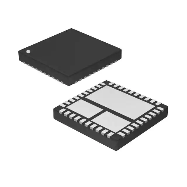
Vishay Siliconix SIC778ACD-T1-GE3

Part No.:
SIC778ACD-T1-GE3
Manufacturer:
Vishay Siliconix
Category:
Full Half-Bridge (H Bridge) Drivers
Package:
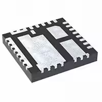
PowerPAK® MLP66-40
Datasheet:
AetrixSIC778ACD-T1-GE3.pdf
Description:
IC HALF BRIDGE DRIVER 40A PPAK
Quantity:
Payment:
Payment
Shipping:
Shipping

Inventory:1,687

Please send an inquiry. Send us your inquiry, and we will respond immediately.

Part Number
Quantity*
Price
Name*
Company
Email*
Comments

Product details

Overview

SIC778ACD-T1-GE3 from Vishay Siliconix is a high-performance DrMOS integrated power stage for synchronous buck converters, featuring 3.3 V PWM logic compatibility, adaptive dead-time control, and integrated bootstrap Schottky diode. It delivers over 40 A continuous current per phase with 91 % peak efficiency at 12 V input and supports switching frequencies up to 1 MHz in CPU/GPU VRD applications.

For engineers reviewing the SIC778ACD-T1-GE3 datasheet, SIC778ACD-T1-GE3 pinout, SIC778ACD-T1-GE3 application, or SIC778ACD-T1-GE3 equivalent, key selection criteria include tri-state PWM support, thermal warning (THDN) flag, SMOD-enabled light-load efficiency, <20 ns PWM propagation delay, and compliance with Intel DrMOS 4.0 specification.

Technical Context

The SIC778ACD-T1-GE3 integrates TrenchFET Gen III MOSFETs optimized for 12 V input stages, with adaptive shoot-through protection that monitors GH/GL gate voltages and enforces ≥1 V threshold before enabling turn-on. Its gate driver supports tri-state PWM logic, SMOD-controlled diode emulation mode, and VCIN/VDRV separate biasing for noise isolation.

It implements an internal thermal monitor with 160 °C trip point and 25 °C hysteresis, open-drain THDN output, plus UVLO on VCIN (4.3 V rising, 3.2 V falling) and DSBL# active-low disable with internal pull-down. The device operates across –40 °C to +125 °C ambient and features 2.5 °C/W junction-to-case thermal resistance via the P3 VSWH pad.

Key Specifications

ParameterValue and Actual Design Meaning
Continuous Current≥40 A per phase - enables high-density multi-phase VRDs without external current sharing
Peak Efficiency91 % at VIN = 12 V, VOUT = 1.2 V - reduces thermal load and improves POL module power density
Max Switching Frequency1 MHz - supports compact filter design with sub-µH inductors in high-speed VR applications
PWM Logic ThresholdRising: 2.4 V typ., Falling: 0.9 V typ. - ensures robust 3.3 V logic interface with hysteresis against noise
Propagation Delay<20 ns (tri-state to GH/GL rise) - preserves tight timing control in high-frequency multi-phase systems
Junction Temp Limit150 °C max - defines safe operating boundary under sustained high-current transient loads
Thermal Resistance θJC2.5 °C/W - enables direct thermal coupling to PCB copper for efficient heat extraction

Pinout & Package

Package: PowerPAK® MLP6x6-40L (6 mm × 6 mm, 40-pin, thermally enhanced QFN-style with exposed VSWH pad).

Pin/TerminalCircuit RoleDesign Meaning
1 (SMOD#)Diode emulation mode controlActive-low input enabling non-synchronous operation to reduce light-load switching losses
2 (VCIN)Logic supply voltageBias for internal control circuitry; UVLO threshold 3.7–4.3 V ensures stable startup
3 (VDRV)Gate driver supplyIndependent 4.5–5.5 V rail for HS/LS drivers; separation from VCIN minimizes noise coupling
4 (BOOT)High-side bootstrap nodeConnects to external capacitor; integrated Schottky eliminates need for external diode
5,37,P1 (CGND)Analog ground referenceReference for driver logic; must be tied externally to PGND with minimal inductance (<0.5 V transient)
6 (GH)High-side gate drive outputDrives HS MOSFET gate; monitored for adaptive dead-time control and shoot-through prevention
7 (PHASE)HS return / BOOT discharge pathInternally connected to VSWH; provides discharge path for GH via 20.2 kΩ resistor when VCIN = 0
8–14,P2 (VIN)Power input / HS drainConnects to 4.5–18 V intermediate bus; rated for –0.3 to 20 V absolute max
15,29–35,P3 (VSWH)Switch node outputPhase node output to LC filter; serves as thermal pad (P3) with θJC = 2.5 °C/W
16–28 (PGND)Power groundLow-inductance return for HS/LS current paths; layout-critical for EMI and stability
36 (GL)Low-side gate drive outputDrives LS MOSFET gate; synchronized with GH using adaptive dead-time logic
38 (THDN)Thermal warning flagOpen-drain output asserting at TJ = 160 °C; clears at 135 °C; requires external pull-up to VCIN
39 (DSBL#)Global disable controlActive-low shutdown; internal pull-down ensures safe default state if left floating
40 (PWM)Tri-state PWM inputAccepts 3.3 V logic with tri-state hold-off (150 ns); supports advanced VR controller sequencing

Key Features

FeatureDesign Value
Adaptive dead-time controlMonitors GH/GL gate voltages in real time and enforces ≥1 V off-state before enabling opposite FET turn-on, eliminating shoot-through risk across temperature and load
Integrated bootstrap Schottky diodeEliminates external diode requirement and reduces BOM count while maintaining reliable high-side gate drive charge pump operation
Tri-state PWM compatibilitySupports advanced VR controllers with high-impedance shutdown states, enabling clean phase disable without negative inductor swing or external clamping
SMOD logic for light-load efficiencyDisables LS FET during discontinuous conduction mode, reducing switching losses and improving efficiency below ~5 A output current
Thermal warning (THDN)Open-drain flag with 25 °C hysteresis alerts system controller at 160 °C junction temp-enables proactive thermal management without forcing shutdown
Intel DrMOS 4.0 complianceFully meets specification requirements for timing, logic thresholds, protection features, and thermal behavior-ensures interoperability in certified CPU/GPU VR platforms

Applications

CPU Voltage Regulator (VRD)GPU Multi-Phase VR

Use Scenario: High-current, low-voltage regulation for modern x86 processors requiring dynamic load steps up to 300 A/µs.

IC Role / Device Role / Timing Role: Per-phase DrMOS power stage executing synchronous buck conversion with tri-state PWM coordination and adaptive dead-time control.

Use Value: Enables 40+ A/phase current handling and 91 % peak efficiency at 1.2 V output, reducing thermal footprint and supporting Intel VR13/VR14 compliance.

Use Scenario: Compact, high-efficiency power delivery for discrete and integrated GPUs with aggressive transient response demands.

IC Role / Device Role / Timing Role: Integrated power stage providing fast gate drive, SMOD-enabled light-load optimization, and THDN-based thermal monitoring per phase.

Use Value: Delivers >40 A/phase with <20 ns propagation delay and 1 MHz switching capability-supports smaller output filters and faster load-step response.

Memory Subsystem POL ModuleServer ASIC Core Rail

Use Scenario: Point-of-load regulation for DDR4/DDR5 memory VDDQ rails requiring tight voltage accuracy and low noise.

IC Role / Device Role / Timing Role: DrMOS stage operating in multi-phase configuration with VCIN/VDRV decoupling to suppress gate-drive noise coupling into analog references.

Use Value: Achieves 91 % efficiency at 1.1 V/20 A with 2.5 °C/W θJC, enabling direct thermal attachment to heatsink-equipped PCBs for memory subsystems.

Use Scenario: High-reliability core voltage regulation for AI accelerators and network processors with extended temperature operation.

IC Role / Device Role / Timing Role: Robust power stage with DSBL#-controlled safe shutdown, UVLO protection, and –40 °C to +125 °C ambient rating.

Use Value: Supports 150 °C max junction temperature and 125 °C max ambient operation-meets industrial server thermal requirements without derating.

Equivalent & Alternatives

The following parts are listed as comparable options for similar DrMOS power stage applications.

Alternative PartTechnical DifferenceApplication DifferenceSelection Advice
IR35201MTRPBF8-pin SOIC package; dual-phase controller with integrated MOSFET drivers but no integrated power FETsRequires external high/low-side MOSFETs; higher board area and layout complexitySelect when system-level flexibility in FET selection or thermal partitioning is prioritized over integration density
MP86957GQZ-1040-pin QFN, 60 A rated, 93 % peak efficiency; supports 3.3 V/5 V PWM logic but lacks THDN flag and tri-state hold-offNo thermal warning output or tri-state PWM sequencing-limits use in Intel-compliant VR platforms requiring DrMOS 4.0Select for higher-current, higher-efficiency applications where THDN and tri-state are not required by platform spec

Compared with IR35201MTRPBF and MP86957GQZ-10, the SIC778ACD-T1-GE3 uniquely combines 40 A capability, Intel DrMOS 4.0 compliance, THDN thermal flag, and tri-state PWM support in a single MLP6x6-40L package-making it optimal for space-constrained, standards-compliant CPU/GPU VR designs.

Availability

SIC778ACD-T1-GE3 is available at Aetrix Electronics and suitable for CPU voltage regulator modules, GPU multi-phase power delivery, and server ASIC core rail applications requiring stable component supply, long-term lifecycle assurance, and traceable sourcing.

Supply support for SIC778ACD-T1-GE3 includes scheduled delivery planning, volume procurement assistance, BOM continuity management, traceable sourcing, and lifecycle availability coordination for OEM customers, industrial embedded developers, connected-device designers, and electronics production programs.

Manufacturer

Vishay Siliconix is a global leader in discrete semiconductors and integrated power solutions, specializing in high-efficiency MOSFETs, diodes, and power stages for computing, industrial, and automotive markets.

The SiC778A product line was designed specifically for high-current, high-frequency synchronous buck applications in CPU/GPU VRDs, emphasizing integration density, thermal performance, and Intel DrMOS 4.0 compliance.

FAQ

What is the maximum continuous output current supported by the SIC778ACD-T1-GE3?

The SIC778ACD-T1-GE3 is rated for over 40 A continuous current per phase under typical conditions (VIN = 12 V, TA = 25 °C, no airflow). Actual achievable current depends on PCB layout, thermal management, and switching frequency-designs with optimized copper area and forced airflow can sustain this rating across full ambient range.

Does the SIC778ACD-T1-GE3 support tri-state PWM inputs, and how does it behave during controller high-impedance states?

Yes, the SIC778ACD-T1-GE3 supports tri-state PWM inputs. When the PWM signal enters high-impedance, the internal circuitry detects the voltage entering the tri-state region (1.8 V nominal) for ≥150 ns (TTSHO), then disables both GH and GL outputs. This prevents negative inductor swing and eliminates need for external Schottky clamps during phase disable sequences.

How does the THDN pin function, and what external components are required for proper operation?

The THDN pin is an open-drain thermal warning output that asserts low when junction temperature exceeds 160 °C and clears at 135 °C. It requires an external pull-up resistor (≤20 kΩ) to VCIN. No additional filtering or buffering is needed-the flag is intended for direct connection to system PMIC or microcontroller GPIO for thermal event logging or throttling decisions.

What is the purpose of separating VCIN and VDRV pins, and how should they be routed on the PCB?

VCIN powers the logic control circuitry, while VDRV supplies the high-current gate drivers. Separating them-typically with a small series resistor (e.g., 1–10 Ω) and local decoupling-creates a low-pass filter that prevents high-frequency gate-switching noise from coupling into the sensitive control logic. This improves noise immunity and timing stability, especially in multi-phase layouts with shared ground planes.

Is the SIC778ACD-T1-GE3 compliant with Intel DrMOS 4.0, and which specific requirements does it meet?

Yes, the SIC778ACD-T1-GE3 is explicitly compliant with Intel DrMOS 4.0. It meets all mandatory requirements including 3.3 V PWM logic thresholds (2.1–2.8 V rising, 0.7–1.2 V falling), tri-state hold-off time (≥150 ns), THDN thermal flag behavior, UVLO thresholds (4.3 V on, 3.2 V off), and adaptive dead-time implementation-verified per specification Document Number 63808 Rev. B.

SIC778ACD-T1-GE3 Specifications

Product attributes
Attribute value
Manufacturer:
Vishay Siliconix
Series:
-
Package/Case:
PowerPAK® MLP66-40
Packaging:
Tape & Reel (TR)
Product Status:
Obsolete
Output Configuration:
Half Bridge
Applications:
Synchronous Buck Converters
Interface:
PWM
Load Type:
Inductive
Technology:
DrMOS
Rds On (Typ):
-
Current - Output / Channel:
40A
Current - Peak Output:
-
Voltage - Supply:
4.5V ~ 5.5V
Voltage - Load:
4.5V ~ 18V
Operating Temperature:
-40°C ~ 150°C (TJ)
Grade:
-
Qualification:
-
Features:
Bootstrap Circuit, Diode Emulation, Status Flag
Fault Protection:
Over Temperature, Shoot-Through, UVLO
Mounting Type:
Surface Mount
Supplier Device Package:
PowerPAK® MLP66-40

SIC778ACD-T1-GE3 FAQ

1.How can I place an order for SIC778ACD-T1-GE3 through Aetrix?

Please submit a Request for Quotation (RFQ) for SIC778ACD-T1-GE3 on Aetrix. Our sales agent will provide a competitive quotation and guide you through the order confirmation once you accept the terms.

2.Are the price and stock information for SIC778ACD-T1-GE3 reliable?

The price and inventory of SIC778ACD-T1-GE3 are updated periodically and may fluctuate due to market conditions. Stock and pricing data are typically refreshed every 24 hours. Quotation validity for SIC778ACD-T1-GE3 is usually 5 days.

3.What payment methods are accepted for SIC778ACD-T1-GE3?

We accept Wire Transfer, PayPal, Credit Card, Western Union, MoneyGram, and Escrow for SIC778ACD-T1-GE3 transactions.

Note: Certain payment methods may incur a processing fee.

4.How is shipping managed for SIC778ACD-T1-GE3?

SIC778ACD-T1-GE3 orders can be shipped via leading logistics carriers, including DHL, UPS, FedEx, TNT, or Registered Mail.

Once your SIC778ACD-T1-GE3 order is processed, you will receive an email with the shipment details and tracking number.

Note: Tracking information may take up to 24 hours to appear. Express delivery typically takes 3–5 business days.

5.How can I obtain technical support or documentation for SIC778ACD-T1-GE3?

For technical support, including SIC778ACD-T1-GE3 datasheets, pinout diagrams, or application guidance, please contact our engineering support team. They can provide detailed documentation and assistance for your SIC778ACD-T1-GE3 requirements.

6.How does Aetrix verify that SIC778ACD-T1-GE3 is sourced from the original manufacturer or authorized distributors?

All SIC778ACD-T1-GE3 products on Aetrix are procured from qualified distributors and authorized channels. Our dedicated quality assurance team conducts strict verification, including traceability checks and, if necessary, third-party testing. This ensures that SIC778ACD-T1-GE3 meets industry standards.

7.What is the process for return or replacement of SIC778ACD-T1-GE3?

All SIC778ACD-T1-GE3 units undergo pre-shipment inspection (PSI). If there is an issue with SIC778ACD-T1-GE3, returns or replacements are accepted under the following conditions:

1.Quantity discrepancies, incorrect items, or visible external defects (such as breakage or corrosion), acknowledged by Aetrix.

2.The issue is reported within 90 days of delivery.

3.The SIC778ACD-T1-GE3 part is unused and in its original packaging.

Return procedure for SIC778ACD-T1-GE3:

1.Submit a request within 90 days.

2.Obtain a Return Material Authorization (RMA) from Aetrix.

SIC778ACD-T1-GE3 Tags

  • SIC778ACD-T1-GE3
  • SIC778ACD-T1-GE3 PDF
  • SIC778ACD-T1-GE3 Datasheet
  • SIC778ACD-T1-GE3 Specifications
  • SIC778ACD-T1-GE3 Images
  • Vishay Siliconix
  • Vishay Siliconix SIC778ACD-T1-GE3
  • Buy SIC778ACD-T1-GE3
  • SIC778ACD-T1-GE3 Price
  • SIC778ACD-T1-GE3 Distributor
  • SIC778ACD-T1-GE3 Supplier
  • SIC778ACD-T1-GE3 Wholesale
Related Products
NCP1393BDR2G
NCP1393BDR2G

onsemi

A3909GLNTR-T
A3909GLNTR-T

Allegro MicroSystems

NCP51530BDR2G
NCP51530BDR2G

onsemi

A3909GLYTR-T
A3909GLYTR-T

Allegro MicroSystems

SIC631CD-T1-GE3
SIC631CD-T1-GE3

Vishay Siliconix

BTN70301EPAXUMA1
BTN70301EPAXUMA1

Infineon Technologies

TDA21520AUMA1
TDA21520AUMA1

Infineon Technologies

AOZ5116QI
AOZ5116QI

Alpha & Omega Semiconductor Inc.
IRSM005-301MHTR
IRSM005-301MHTR

Infineon Technologies

IRSM005-301MH
IRSM005-301MH

Infineon Technologies

MP6610GJ-Z
MP6610GJ-Z

Monolithic Power Systems Inc.

DRV8908QPWPRQ1
DRV8908QPWPRQ1

Texas Instruments

Tech Hub

Search

Search

PRODUCT

PRODUCT

PHONE

PHONE

USER

USER