
 My Inquiry
 My Account


Asahi Kasei Microdevices/AKM AP1014AEC
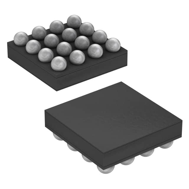
- Part No.:
- AP1014AEC
- Manufacturer:
- Asahi Kasei Microdevices/AKM
- Category:
- Full Half-Bridge (H Bridge) Drivers
- Package:
- 16-UFBGA, WLCSP
- Datasheet:
-
 AP1014AEC.pdf
- Description:
- IC HALF BRIDGE DRVR 1.1A 16WLCSP
- Quantity:
- Payment:

- Shipping:

Inventory:4,785
Please send an inquiry. Send us your inquiry, and we will respond immediately.
Product details
Overview
AP1014AEC from Asahi Kasei Microdevices is a dual H-bridge motor driver IC integrating N-channel LDMOS FETs on both high-side and low-side outputs, supporting forward/reverse/brake/standby modes with 7.0V motor supply, 2.7–5.5V control supply, and 1.1A DC output per channel at 25°C. It enables PWM-driven small-motor control in space-constrained applications.
For engineers reviewing the AP1014AEC datasheet, AP1014AEC pinout, AP1014AEC application, or AP1014AEC equivalent, key selection factors include its WL-CSP package footprint (1.96mm × 1.96mm), SEL-configurable input logic, integrated UVLO (2.2V threshold) and thermal shutdown (175°C), and dual-channel RON of 0.35Ω (typ) at 25°C.
Technical Context
The AP1014AEC implements two independent H-bridge drivers with charge-pump-based gate drive for N-ch LDMOS FETs, enabling full-bridge operation without external high-side drivers. Its internal logic supports four motion states-forward, reverse, brake, and standby-via EN, SEL, and dual INnA/INnB inputs per channel.
It integrates under-voltage lockout (VC < 2.2V) and thermal shutdown (Tj = 175°C with 30°C hysteresis), and features separate VM1/VM2 power rails shorted internally, plus GND1/GND2 tied together. The SEL pin selects between active-high and active-low input logic mapping for PWM compatibility.
Key Specifications
| Parameter | Value and Actual Design Meaning |
|---|---|
| Motor Supply Range | 2.0V to 7.0V - Supports battery-powered micro-motor systems including single-cell Li-ion (3.0–4.2V) and dual-cell alkaline (2.4–3.2V). |
| Control Supply Range | 2.7V to 5.5V - Compatible with standard logic domains (3.3V or 5V microcontrollers). |
| Max Output Current (DC) | 1.1A/ch @ 25°C - Sustains continuous drive for small DC motors up to ~1W at 5V. |
| H-Bridge RON (TOP+BOT) | 0.35Ω (typ) @ 25°C - Limits conduction loss to ≤385mW per channel at 1.1A, reducing thermal load in WL-CSP package. |
| UVLO Threshold | 2.2V (typ) on VC - Prevents erratic operation during brown-out conditions in low-voltage control rails. |
| Thermal Shutdown | 175°C (Tj) with 30°C hysteresis - Enables safe recovery after overtemperature events without manual reset. |
| Package | 16-pin WL-CSP (1.96mm × 1.96mm) - Ultra-compact chip-scale packaging for ultra-thin portable devices. |
Pinout & Package
AP1014AEC uses a 16-pin Wafer-Level Chip-Scale Package (WL-CSP) measuring 1.96mm × 1.96mm with 0.5mm pitch and bottom-solder ball layout. Pin assignment follows standard top-view orientation with A1 as reference corner.
| Pin/Terminal | Circuit Role | Design Meaning |
|---|---|---|
| A1 (IN1B) | Input logic signal | Channel 1 bridge control input; logic level defines OUT1B state when EN=H and SEL configured. |
| A2 (IN1A) | Input logic signal | Channel 1 bridge control input; paired with IN1B to determine forward/reverse/brake mode. |
| A3 (VM1) | Motor power rail | Primary motor supply input for Channel 1; internally shorted to VM2 for dual-channel shared supply. |
| A4 (OUT1A) | H-bridge output | High-side output terminal of Channel 1 H-bridge; connects directly to one motor terminal. |
| B1 (GND2) | Power ground | Ground return for Channel 2; internally connected to GND1 for common ground reference. |
| B2 (VG) | Charge pump output | Boosted gate-drive voltage (VC + VM); requires 0.1μF ceramic capacitor to GND for stable operation. |
| B3 (SEL) | Logic configuration | Selects input logic polarity (active-high vs. active-low); internal 200kΩ pull-down ensures default safe state. |
| B4 (OUT1B) | H-bridge output | Low-side output terminal of Channel 1 H-bridge; completes current path through motor winding. |
| C1 (VC) | Control supply | 3.3V/5V logic supply for internal logic and gate drivers; decoupled with 0.1–1.0μF capacitor. |
| C2 (IN2A) | Input logic signal | Channel 2 bridge control input; functionally identical to IN1A but for second motor or coil. |
| C3 (EN) | Enable control | Global enable/disable; internal 200kΩ pull-down ensures Hi-Z output state on power-up. |
| C4 (GND1) | Power ground | Ground return for Channel 1; internally shorted to GND2 for unified ground plane. |
| D1 (IN2B) | Input logic signal | Channel 2 bridge control input; used with IN2A to configure motion direction and braking. |
| D2 (VM2) | Motor power rail | Motor supply input for Channel 2; electrically tied to VM1 inside IC for single-supply operation. |
| D3 (OUT2A) | H-bridge output | High-side output of Channel 2 H-bridge; drives second motor or differential winding pair. |
| D4 (OUT2B) | H-bridge output | Low-side output of Channel 2 H-bridge; complements OUT2A to complete bidirectional drive path. |
Key Features
| Feature | Design Value |
|---|---|
| Dual independent H-bridges | Enables simultaneous bidirectional control of two small DC motors or one stepper motor phase pair. |
| Integrated N-ch LDMOS FETs | Eliminates need for external MOSFETs and gate drivers, reducing BOM count and PCB area in compact designs. |
| SEL-configurable input logic | Allows direct interface with either active-high or active-low PWM controllers without external inverters. |
| Built-in charge pump | Generates boosted gate voltage (VC + VM) to fully enhance high-side N-FETs using only N-channel devices. |
| Thermal shutdown with hysteresis | Prevents latch-up during overload; 30°C hysteresis ensures stable re-enable after cooling without oscillation. |
Applications
| Smartphone Camera Actuators | Wearable Haptic Feedback |
|---|---|
Use Scenario: Driving voice-coil actuators (VCAs) for auto-focus and optical image stabilization (OIS) in smartphone camera modules. IC Role / Device Role / Timing Role: Dual H-bridge provides precise bidirectional current control to VCA coils with sub-millisecond response and low quiescent current in standby. Use Value: Enables 1.1A peak drive capability and 0.35Ω RON to achieve fast lens positioning while minimizing heat generation in thermally constrained camera assemblies. | Use Scenario: Powering eccentric rotating mass (ERM) or linear resonant actuator (LRA) motors in smartwatches and fitness bands. IC Role / Device Role / Timing Role: Delivers programmable PWM-controlled vibration intensity via configurable input logic and fast propagation delay (<0.5μs). Use Value: SEL pin simplifies firmware integration with existing MCU GPIO mappings; WL-CSP package fits within <2mm board height budgets. |
| Medical Drug Delivery Pumps | Miniature Robotics Joints |
Use Scenario: Controlling micro-peristaltic or syringe-pump DC motors in portable insulin or infusion pumps. IC Role / Device Role / Timing Role: Provides fault-protected motor drive with UVLO and thermal shutdown, ensuring fail-safe stop during low-battery or overheating conditions. Use Value: 2.0V–7.0V motor supply range supports single- or dual-cell battery configurations; 1.1A DC rating handles typical 0.5–1.0W pump loads. | Use Scenario: Driving geared DC motors in palm-sized robotic platforms requiring dual-axis motion (e.g., pan/tilt, gripper/wrist). IC Role / Device Role / Timing Role: Dual-channel H-bridge replaces two discrete drivers, reducing component count and interconnect complexity in multi-joint control. Use Value: Shared VM/GND rails simplify power routing; compact WL-CSP allows placement near motor connectors to minimize trace inductance. |
Equivalent & Alternatives
The following parts are listed as comparable options for similar dual H-bridge motor driver applications.
| Alternative Part | Technical Difference | Application Difference | Selection Advice |
|---|---|---|---|
| TB67H420FTG | Higher 2.0A DC rating per channel; larger HTSOP-J8 package (4.0mm × 4.0mm); no SEL pin for logic inversion. | Better suited for higher-current motors (>1.1A) where board space permits larger footprint. | Choose TB67H420FTG when thermal headroom and peak current demand exceed AP1014AEC limits. |
| DRV8837C | Single H-bridge; 1.8A peak; 6-pin WSON package; no charge pump (requires external high-side driver or P-FET). | Requires two units for dual-channel operation; lacks integrated gate boost and SEL flexibility. | Select DRV8837C only for cost-sensitive single-motor applications where dual-channel integration is unnecessary. |
Compared with TB67H420FTG and DRV8837C, the AP1014AEC uniquely combines dual-channel integration, SEL-configurable logic, and WL-CSP packaging-enabling space-constrained, low-power bidirectional motor control without external gate drivers or logic inverters.
Availability
AP1014AEC is available at Aetrix Electronics and suitable for smartphone camera modules, wearable haptics, medical drug delivery pumps, and miniature robotics requiring stable component supply and long-term lifecycle support.
Supply support for AP1014AEC includes scheduled delivery planning, volume procurement assistance, BOM continuity management, traceable sourcing, and lifecycle availability coordination for OEM customers, industrial embedded developers, connected-device designers, and electronics production programs.
Manufacturer
Asahi Kasei Microdevices (AKM) is a Japanese semiconductor company specializing in analog, mixed-signal, and sensor ICs, with core expertise in audio, motor control, and magnetic sensing technologies.
The AP1014AEC belongs to AKM's motor driver product line, designed specifically for ultra-compact, low-voltage bidirectional motor control in portable and wearables applications where size, thermal efficiency, and logic flexibility are critical.
FAQ
What is the maximum continuous output current per channel for the AP1014AEC?
The AP1014AEC delivers 1.1A DC per channel at Ta = 25°C and 0.8A per channel at Ta = 85°C. These values reflect actual thermal derating under sustained load; peak current capability reaches 2.0A for pulses ≤10ms within a 200ms window. Designers must verify PCB copper area and airflow to maintain these ratings in end equipment.
Does the AP1014AEC require external components for gate driving?
No-the AP1014AEC integrates a charge pump circuit that generates VG = VC + VM to fully enhance its internal N-channel LDMOS high-side FETs. Only a 0.1μF ceramic capacitor between VG and GND is required. No external gate drivers, bootstrap circuits, or high-side P-FETs are needed, simplifying design and reducing bill-of-materials.
How does the SEL pin affect input logic behavior in the AP1014AEC?
The SEL pin configures whether the AP1014AEC interprets INnA/INnB as active-high or active-low signals. When SEL = L, inputs follow standard active-high logic; when SEL = H, they invert-allowing seamless interface with MCUs that lack configurable GPIO polarity. An internal 200kΩ pull-down ensures safe default (SEL = L) at power-up.
What protection features are built into the AP1014AEC?
The AP1014AEC includes under-voltage lockout (UVLO) that disables operation if VC drops below 2.2V, and thermal shutdown that activates at Tj = 175°C with 30°C hysteresis. Both functions are fully internal-no external components or configuration are required. These protections prevent malfunction during brown-out or overload conditions, enhancing system reliability.
Is the AP1014AEC compatible with 3.3V microcontroller GPIOs?
Yes-the AP1014AEC accepts control inputs (INnA, INnB, EN, SEL) referenced to VC, which operates from 2.7V to 5.5V. With VC = 3.3V, VIH ≥ 2.31V and VIL ≤ 0.99V, making it fully compatible with standard 3.3V CMOS logic. Input leakage remains below ±21μA, ensuring minimal loading on MCU outputs.
AP1014AEC Specifications
- Product attributes
- Attribute value
- Manufacturer:
- Asahi Kasei Microdevices/AKM
- Series:
- -
- Package/Case:
- 16-UFBGA, WLCSP
- Packaging:
- Tape & Reel (TR)
- Product Status:
- Not For New Designs
- Output Configuration:
- Half Bridge (4)
- Applications:
- General Purpose
- Interface:
- Logic
- Load Type:
- Inductive
- Technology:
- Power MOSFET
- Rds On (Typ):
- 350mOhm LS + HS
- Current - Output / Channel:
- 1.1A
- Current - Peak Output:
- 2A
- Voltage - Supply:
- 2.7V ~ 5.5V
- Voltage - Load:
- 2V ~ 7V
- Operating Temperature:
- -30°C ~ 150°C (TJ)
- Grade:
- -
- Qualification:
- -
- Features:
- -
- Fault Protection:
- Over Temperature, UVLO
- Mounting Type:
- Surface Mount
- Supplier Device Package:
- 16-WLCSP (1.96x1.96)
AP1014AEC FAQ
1.How can I place an order for AP1014AEC through Aetrix?
Please submit a Request for Quotation (RFQ) for AP1014AEC on Aetrix. Our sales agent will provide a competitive quotation and guide you through the order confirmation once you accept the terms.
2.Are the price and stock information for AP1014AEC reliable?
The price and inventory of AP1014AEC are updated periodically and may fluctuate due to market conditions. Stock and pricing data are typically refreshed every 24 hours. Quotation validity for AP1014AEC is usually 5 days.
3.What payment methods are accepted for AP1014AEC?
We accept Wire Transfer, PayPal, Credit Card, Western Union, MoneyGram, and Escrow for AP1014AEC transactions.
Note: Certain payment methods may incur a processing fee.
4.How is shipping managed for AP1014AEC?
AP1014AEC orders can be shipped via leading logistics carriers, including DHL, UPS, FedEx, TNT, or Registered Mail.
Once your AP1014AEC order is processed, you will receive an email with the shipment details and tracking number.
Note: Tracking information may take up to 24 hours to appear. Express delivery typically takes 3–5 business days.
5.How can I obtain technical support or documentation for AP1014AEC?
For technical support, including AP1014AEC datasheets, pinout diagrams, or application guidance, please contact our engineering support team. They can provide detailed documentation and assistance for your AP1014AEC requirements.
6.How does Aetrix verify that AP1014AEC is sourced from the original manufacturer or authorized distributors?
All AP1014AEC products on Aetrix are procured from qualified distributors and authorized channels. Our dedicated quality assurance team conducts strict verification, including traceability checks and, if necessary, third-party testing. This ensures that AP1014AEC meets industry standards.
7.What is the process for return or replacement of AP1014AEC?
All AP1014AEC units undergo pre-shipment inspection (PSI). If there is an issue with AP1014AEC, returns or replacements are accepted under the following conditions:
1.Quantity discrepancies, incorrect items, or visible external defects (such as breakage or corrosion), acknowledged by Aetrix.
2.The issue is reported within 90 days of delivery.
3.The AP1014AEC part is unused and in its original packaging.
Return procedure for AP1014AEC:
1.Submit a request within 90 days.
2.Obtain a Return Material Authorization (RMA) from Aetrix.
AP1014AEC Tags

-
NCP1393BDR2G
onsemi
-
A3909GLNTR-T
Allegro MicroSystems
-
NCP51530BDR2G
onsemi
-
A3909GLYTR-T
Allegro MicroSystems
-
SIC631CD-T1-GE3
Vishay Siliconix
-
BTN70301EPAXUMA1
Infineon Technologies

-
TDA21520AUMA1
Infineon Technologies
-
AOZ5116QI
Alpha & Omega Semiconductor Inc.
-
IRSM005-301MHTR
Infineon Technologies
-
IRSM005-301MH
Infineon Technologies
-
MP6610GJ-Z
Monolithic Power Systems Inc.

-
DRV8908QPWPRQ1
Texas Instruments
Tech Hub

A practical engineering and sourcing framework covering lifecycle verification, lifetime-buy calculations, replacement qualification, supplier checks and counterfeit-risk controls.

TTL and CMOS logic families differ in thresholds, loading, output drive, power and timing. This engineering guide compares 74HC and 74HCT, calculates noise margins and checks 3.3 V/5 V compatibility.

A practical engineering guide to 3.3V and 5V logic compatibility, input thresholds, resistor dividers, translator ICs, MOSFET level shifting, I2C pull-ups, timing limits and power-sequencing risks.

The 74HC595 uses push-pull logic outputs, while the TPIC6B595 uses 50 V open-drain DMOS sinks for higher-power loads. This guide compares timing, current limits, 3.3 V interfacing, load wiring, thermal…

The 74HC595 converts serial data into eight stable parallel outputs. This guide covers pin functions, shift and storage timing, OE and MR behavior, drive-current limits, cascading, voltage compatibilit…

A technical comparison of level-sensitive latches and edge-triggered flip-flops, covering timing windows, setup and hold limits, master–slave operation, time borrowing, race-through, HDL inference and…

A D latch stores one bit while Enable controls when data can pass. This reference covers gate-level operation, truth tables, transparency, setup and hold timing, LE versus OE, common ICs and practical …

An SR latch stores one bit through cross-coupled feedback. This engineering reference covers NOR and NAND implementations, truth tables, forbidden-state recovery, gated operation, switch debouncing, fa…

Latch circuits retain one bit through feedback. This technical reference covers SR and D latches, truth tables, transparency, timing limits, latch-versus-flip-flop behavior, applications and common log…

An engineering guide to LED driver operation, constant-current and constant-voltage outputs, linear and switching topologies, dimming, IC selection, calculations, replacement compatibility, and fault c…


