
 My Inquiry
 My Account


Renesas ISL55111IRZ-T
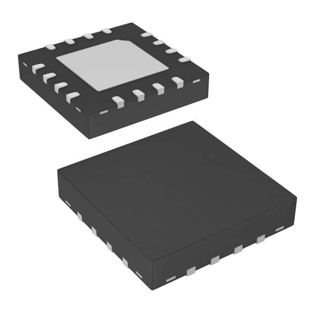
- Part No.:
- ISL55111IRZ-T
- Manufacturer:
- Renesas
- Category:
- Full Half-Bridge (H Bridge) Drivers
- Package:
- 16-TFQFN Exposed Pad
- Datasheet:
-
 ISL55111IRZ-T.pdf
- Description:
- IC HALF BRIDGE DRVR 100MA 16QFN
- Quantity:
- Payment:

- Shipping:

Inventory:11,970
Please send an inquiry. Send us your inquiry, and we will respond immediately.
Product details
Overview
ISL55111IRZ-T from Renesas Electronics is a dual high-speed anti-phase MOSFET driver optimized for accurate pulse generation and low-skew buffering in demanding imaging and timing systems. It delivers 3.5A peak output current, 1.5ns rise/fall times (100pF), 6ns minimum pulse width, and operates with VH = 5–13.2V and VDD = 2.7–5.5V - enabling precise drive of CCD horizontal shift registers and ultrasound transducer arrays.
For engineers reviewing the ISL55111IRZ-T datasheet, ISL55111IRZ-T pinout, ISL55111IRZ-T application, or ISL55111IRZ-T equivalent, this page provides verified functional identity, QFN-16 package mapping, anti-phase output behavior, thermal pad grounding requirement, and validated alternatives for ultrasound, CCD, and clock generation designs.
Technical Context
The ISL55111IRZ-T implements two independent CMOS drivers with complementary (anti-phase) output logic: IN-B is inverted while IN-A is non-inverted, enabling push-pull or differential timing control. Its input stage features tightly controlled hysteresis (0.2V) and logic thresholds (VIX_LH = 1.42V typ, VIX_HL = 1.22V typ) to minimize pulse-width distortion from slow input edges.
Output stage architecture uses rail-to-rail swing between GND and VH with low rDS(on) (3–6Ω), supporting fast switching into capacitive loads up to 680pF while maintaining <0.5ns channel-to-channel skew across -40°C to +85°C. Power-down (PD) and ENABLE pins provide dual-level control: PD reduces quiescent current to 12µA, while ENABLE (QFN-only) tri-states outputs without affecting internal logic.
Key Specifications
| Parameter | Value and Actual Design Meaning |
|---|---|
| VH Supply Range | 5V to 13.2V - sets maximum output voltage swing; enables direct drive of 12V MOSFET gates without level-shifting. |
| Peak Output Current | 3.5A - sustains fast edge rates into heavy capacitive loads (e.g., 330pF CCD lines) without droop or distortion. |
| Rise/Fall Time | 1.2ns/1.4ns @ 100pF - ensures sub-nanosecond timing precision critical for high-resolution ultrasound beamforming. |
| Min Pulse Width | 6ns - supports ultra-short gating pulses required in time-of-flight piezoelectric sensing. |
| Channel Skew | <0.5ns - guarantees matched propagation delay between OA and OB outputs for synchronized dual-channel timing. |
| Logic Compatibility | 3.3V/5V - interfaces directly with FPGA I/O, microcontroller GPIO, and ASIC control logic without external translators. |
| Operating Temp | -40°C to +85°C - qualified for industrial and medical equipment environments including portable ultrasound systems. |
Pinout & Package
ISL55111IRZ-T is supplied in a 16-lead 4×4 mm Exposed Pad QFN package (PKG DWG L16.4x4A). The exposed thermal pad (EP) is electrically connected to GND (Pin 11) and must be soldered to a PCB ground plane for thermal and electrical integrity.
| Pin/Terminal | Circuit Role | Design Meaning |
|---|---|---|
| VDD (Pin 1) | Logic supply input | Powers internal input buffer and control logic; accepts 2.7–5.5V; requires local 0.1µF + 4.7µF bypassing. |
| VH (Pin 10) | Driver high-rail supply | Sets output high-voltage level (5–13.2V); supplies peak current to OA/OB; requires dedicated low-ESR bulk + ceramic decoupling. |
| GND (Pin 11) | Common reference | Returns both VDD and VH currents; tied internally to EP; must connect to solid ground plane to minimize noise coupling and skew. |
| PD (Pin 3) | Power-down enable | Active-high signal reducing total supply current to 12µA (IDD-PDN) + 2.5µA (IH_PDN); used for standby in battery-powered devices. |
| ENABLE (Pin 2) | Output tri-state control | QFN-only pin; low = normal operation, high = OA/OB forced high-impedance - enables dynamic bus sharing or fault isolation. |
| IN-A (Pin 5) | Non-inverting input | Directly controls OA output state (OA = IN-A); compatible with TTL/CMOS logic; rise/fall time <2ns recommended. |
| IN-B (Pin 4) | Inverting input | Controls OB output with inversion (OB = NOT IN-B); establishes anti-phase relationship essential for push-pull gate drive. |
| OA (Pin 9) | Driver A output | High-current CMOS output swinging from GND to VH; capable of sourcing/sinking 3.5A peak; connects to MOSFET gate or load. |
| OB (Pin 12) | Driver B output | Complementary output to OA; anti-phase behavior enables differential signaling, H-bridge pre-drive, or CCD phase clocks. |
Key Features
| Feature | Design Value |
|---|---|
| Anti-phase dual outputs | IN-B inversion ensures precise complementary timing between OA and OB - eliminates external inverters in push-pull or clock-phase applications. |
| Low-output impedance | rDS(on) = 3–6Ω at VH = 12V - minimizes voltage drop under 3.5A peak load, preserving signal fidelity across wide temperature range. |
| Tightly controlled input thresholds | VIX_LH = 1.42V ±0.1V, VIX_HL = 1.22V ±0.1V - suppresses pulse-width jitter caused by slow input transitions in noisy digital environments. |
| Integrated power-down and tri-state | Separate PD and ENABLE pins allow hierarchical control: PD saves power globally; ENABLE isolates outputs dynamically during system reconfiguration. |
| Thermally enhanced QFN | θJA = 45°C/W with proper PCB layout - enables sustained 50MHz operation into 330pF loads without exceeding +150°C junction limit. |
Applications
| Ultrasound Transducer Driver | CCD Horizontal Shift Register |
|---|---|
|
Use Scenario: Driving high-voltage piezoelectric elements in portable ultrasound probes requiring precise 5–12V pulsing at 1–10MHz. IC Role / Device Role / Timing Role: Dual anti-phase gate driver generating complementary HV pulses to excite transmit/receive transducer pairs with sub-ns timing alignment. Use Value: 6ns minimum pulse width and <0.5ns skew ensure clean acoustic pulse generation and echo sampling resolution down to 1mm. |
Use Scenario: Clocking horizontal pixel shift registers in large-format CCD image sensors used in medical endoscopes and industrial inspection cameras. IC Role / Device Role / Timing Role: High-current, low-skew dual driver delivering precisely timed, rail-to-rail clock phases (Φ1/Φ2) to advance charge packets across 4K+ pixel rows. Use Value: 1.5ns rise/fall times and 3.5A peak drive sustain fast settling into 330pF+ line capacitance, enabling >30fps full-frame readout. |
| Clock Generation Circuit | Piezoelectric Distance Sensor |
|
Use Scenario: Generating high-fidelity, low-jitter clock signals for high-speed ADCs, DACs, or FPGA-based signal processing in test equipment. IC Role / Device Role / Timing Role: Buffering and amplifying low-voltage logic clocks to robust 12V CMOS levels while preserving edge integrity and phase relationship. Use Value: 5V–13.2V VH range and 3.5A drive capability eliminate need for discrete level-shifting stages, reducing board area and signal path complexity. |
Use Scenario: Driving resonant piezoelectric transducers in industrial distance measurement systems operating at 40–200kHz with µs-level timing accuracy. IC Role / Device Role / Timing Role: Delivering short, high-amplitude voltage pulses to excite transducers and generate acoustic bursts for time-of-flight calculation. Use Value: 6ns minimum pulse width and tight input hysteresis ensure consistent burst duration and minimal jitter - critical for ±0.1mm measurement repeatability. |
Equivalent & Alternatives
The following parts are listed as comparable options for similar dual anti-phase MOSFET driver applications.
| Alternative Part | Technical Difference | Application Difference | Selection Advice |
|---|---|---|---|
| IXDD614PI | Single-channel, 4A peak, no ENABLE pin, SOIC-8 package; lacks anti-phase logic - requires external inverter for dual complementary output. | Best suited for space-constrained single-output gate drive; not drop-in for dual anti-phase timing-critical systems like CCD clocks. | Select when only one high-current output is needed and board layout favors SOIC; verify timing skew manually if paired with external inverter. |
| LM5112MYX/NOPB | Dual non-inverting driver (no built-in inversion), 5A peak, 12V max VH, WSON-8; includes adjustable dead-time control but no PD or ENABLE. | Targeted at synchronous buck gate drive; lacks native anti-phase mode - unsuitable for CCD horizontal clocks or ultrasound transmit/receive phasing. | Prefer for power converter half-bridge pre-drive where independent control of both FETs is required; avoid for imaging timing applications needing inherent complementarity. |
Compared with IXDD614PI and LM5112MYX/NOPB, the ISL55111IRZ-T uniquely integrates anti-phase logic, ENABLE tri-state, and power-down in a thermally optimized QFN - making it the only choice for compact, low-skew, multi-mode imaging and precision timing systems.
Availability
ISL55111IRZ-T is available at Aetrix Electronics and suitable for ultrasound imaging systems, CCD camera modules, and high-frequency clock generation circuits requiring stable component supply, RoHS-compliant packaging, and guaranteed -40°C to +85°C operation.
Supply support for ISL55111IRZ-T includes scheduled delivery planning, volume procurement assistance, BOM continuity management, traceable sourcing, and lifecycle availability coordination for OEM customers, industrial embedded developers, connected-device designers, and electronics production programs.
Manufacturer
Renesas Electronics is a global semiconductor leader specializing in microcontrollers, analog, power, and mixed-signal solutions for industrial, automotive, and healthcare applications.
The ISL55111IRZ-T belongs to Renesas' high-speed driver product line, engineered specifically for precision pulse generation in medical imaging, scientific instrumentation, and high-resolution sensing systems where timing accuracy and output fidelity are critical.
FAQ
What is the function of the ENABLE pin on the ISL55111IRZ-T?
The ENABLE pin (Pin 2) is exclusive to the QFN package and provides hardware-level output tri-state control. When ENABLE is driven high, both OA and OB outputs enter high-impedance state regardless of IN-A/IN-B states - enabling dynamic bus sharing, fault containment, or safe hot-plug operation. ISL55111IRZ-T requires ENABLE to be pulled low for normal anti-phase driver operation.
Does the ISL55111IRZ-T support 3.3V logic inputs with a 12V VH supply?
Yes. The ISL55111IRZ-T is fully compatible with 3.3V logic families across its specified VDD range (2.7–5.5V). Input thresholds (VIX_LH = 1.42V typ, VIX_HL = 1.22V typ) and hysteresis (0.2V) ensure reliable switching even with marginal 3.3V signals, while VH = 12V allows full rail-to-rail output swing - a key capability of the ISL55111IRZ-T in mixed-voltage systems.
How does the anti-phase functionality of the ISL55111IRZ-T differ from the ISL55110?
The ISL55111IRZ-T has an inverted IN-B input, causing OB to be the logical complement of IN-B, while OA follows IN-A directly - producing inherently anti-phase outputs. In contrast, the ISL55110 drives both OA and OB non-inverted, yielding in-phase outputs. This architectural difference makes ISL55111IRZ-T ideal for push-pull, differential clocking, or CCD Φ1/Φ2 generation without external logic.
What is the correct PCB layout practice for the exposed thermal pad on the ISL55111IRZ-T?
The exposed pad (EP) of the ISL55111IRZ-T is electrically connected to GND (Pin 11) and must be soldered to a solid PCB ground plane using a minimum 9×9 array of thermal vias (0.3mm diameter, 0.8mm pitch) to a dedicated inner-layer ground plane. This ensures both thermal dissipation (θJA = 45°C/W) and low-inductance return path - critical for minimizing ground bounce and skew in high-speed operation of the ISL55111IRZ-T.
Can the ISL55111IRZ-T drive a 680pF capacitive load while maintaining specified timing performance?
Yes. The ISL55111IRZ-T is characterized for CL = 680pF loads: tR = 6.2ns and tF = 6.9ns (typical, VH = 12V, VDD = 3.6V), with tpdR/tpdF ≤14.5ns and skew <0.5ns. These values are measured per Figure 3 in the FN6228 datasheet and confirmed over -40°C to +85°C - validating ISL55111IRZ-T for large-area CCD arrays and high-density bus driving where load capacitance exceeds 500pF.
ISL55111IRZ-T Specifications
- Product attributes
- Attribute value
- Manufacturer:
- Renesas
- Series:
- -
- Package/Case:
- 16-TFQFN Exposed Pad
- Packaging:
- Tape & Reel (TR)
- Product Status:
- Active
- Output Configuration:
- Half Bridge (2)
- Applications:
- Digital Imaging
- Interface:
- Logic
- Load Type:
- Capacitive and Resistive
- Technology:
- Power MOSFET
- Rds On (Typ):
- 3Ohm
- Current - Output / Channel:
- 100mA
- Current - Peak Output:
- 3.5A
- Voltage - Supply:
- 2.7V ~ 5.5V
- Voltage - Load:
- 5V ~ 13.2V
- Operating Temperature:
- -40°C ~ 150°C (TJ)
- Grade:
- -
- Qualification:
- -
- Features:
- -
- Fault Protection:
- -
- Mounting Type:
- Surface Mount
- Supplier Device Package:
- 16-QFN (4x4)
ISL55111IRZ-T FAQ
1.How can I place an order for ISL55111IRZ-T through Aetrix?
Please submit a Request for Quotation (RFQ) for ISL55111IRZ-T on Aetrix. Our sales agent will provide a competitive quotation and guide you through the order confirmation once you accept the terms.
2.Are the price and stock information for ISL55111IRZ-T reliable?
The price and inventory of ISL55111IRZ-T are updated periodically and may fluctuate due to market conditions. Stock and pricing data are typically refreshed every 24 hours. Quotation validity for ISL55111IRZ-T is usually 5 days.
3.What payment methods are accepted for ISL55111IRZ-T?
We accept Wire Transfer, PayPal, Credit Card, Western Union, MoneyGram, and Escrow for ISL55111IRZ-T transactions.
Note: Certain payment methods may incur a processing fee.
4.How is shipping managed for ISL55111IRZ-T?
ISL55111IRZ-T orders can be shipped via leading logistics carriers, including DHL, UPS, FedEx, TNT, or Registered Mail.
Once your ISL55111IRZ-T order is processed, you will receive an email with the shipment details and tracking number.
Note: Tracking information may take up to 24 hours to appear. Express delivery typically takes 3–5 business days.
5.How can I obtain technical support or documentation for ISL55111IRZ-T?
For technical support, including ISL55111IRZ-T datasheets, pinout diagrams, or application guidance, please contact our engineering support team. They can provide detailed documentation and assistance for your ISL55111IRZ-T requirements.
6.How does Aetrix verify that ISL55111IRZ-T is sourced from the original manufacturer or authorized distributors?
All ISL55111IRZ-T products on Aetrix are procured from qualified distributors and authorized channels. Our dedicated quality assurance team conducts strict verification, including traceability checks and, if necessary, third-party testing. This ensures that ISL55111IRZ-T meets industry standards.
7.What is the process for return or replacement of ISL55111IRZ-T?
All ISL55111IRZ-T units undergo pre-shipment inspection (PSI). If there is an issue with ISL55111IRZ-T, returns or replacements are accepted under the following conditions:
1.Quantity discrepancies, incorrect items, or visible external defects (such as breakage or corrosion), acknowledged by Aetrix.
2.The issue is reported within 90 days of delivery.
3.The ISL55111IRZ-T part is unused and in its original packaging.
Return procedure for ISL55111IRZ-T:
1.Submit a request within 90 days.
2.Obtain a Return Material Authorization (RMA) from Aetrix.
ISL55111IRZ-T Tags

-
NCP1393BDR2G
onsemi
-
A3909GLNTR-T
Allegro MicroSystems
-
NCP51530BDR2G
onsemi
-
A3909GLYTR-T
Allegro MicroSystems
-
SIC631CD-T1-GE3
Vishay Siliconix
-
BTN70301EPAXUMA1
Infineon Technologies

-
TDA21520AUMA1
Infineon Technologies
-
AOZ5116QI
Alpha & Omega Semiconductor Inc.
-
IRSM005-301MHTR
Infineon Technologies
-
IRSM005-301MH
Infineon Technologies
-
MP6610GJ-Z
Monolithic Power Systems Inc.

-
DRV8908QPWPRQ1
Texas Instruments
Tech Hub

TTL and CMOS logic families differ in thresholds, loading, output drive, power and timing. This engineering guide compares 74HC and 74HCT, calculates noise margins and checks 3.3 V/5 V compatibility.

A practical engineering guide to 3.3V and 5V logic compatibility, input thresholds, resistor dividers, translator ICs, MOSFET level shifting, I2C pull-ups, timing limits and power-sequencing risks.

The 74HC595 uses push-pull logic outputs, while the TPIC6B595 uses 50 V open-drain DMOS sinks for higher-power loads. This guide compares timing, current limits, 3.3 V interfacing, load wiring, thermal…

The 74HC595 converts serial data into eight stable parallel outputs. This guide covers pin functions, shift and storage timing, OE and MR behavior, drive-current limits, cascading, voltage compatibilit…

A technical comparison of level-sensitive latches and edge-triggered flip-flops, covering timing windows, setup and hold limits, master–slave operation, time borrowing, race-through, HDL inference and…

A D latch stores one bit while Enable controls when data can pass. This reference covers gate-level operation, truth tables, transparency, setup and hold timing, LE versus OE, common ICs and practical …

An SR latch stores one bit through cross-coupled feedback. This engineering reference covers NOR and NAND implementations, truth tables, forbidden-state recovery, gated operation, switch debouncing, fa…

Latch circuits retain one bit through feedback. This technical reference covers SR and D latches, truth tables, transparency, timing limits, latch-versus-flip-flop behavior, applications and common log…

An engineering guide to LED driver operation, constant-current and constant-voltage outputs, linear and switching topologies, dimming, IC selection, calculations, replacement compatibility, and fault c…

Operational amplifier guide covering op amp basics, feedback, ideal vs real op amps, common configurations, buffer circuits, offset, bias current, gain-bandwidth, slew rate, rail-to-rail limits and sel…


