
 My Inquiry
 My Account


Toshiba Semiconductor and Storage TB67Z800FTG,EL
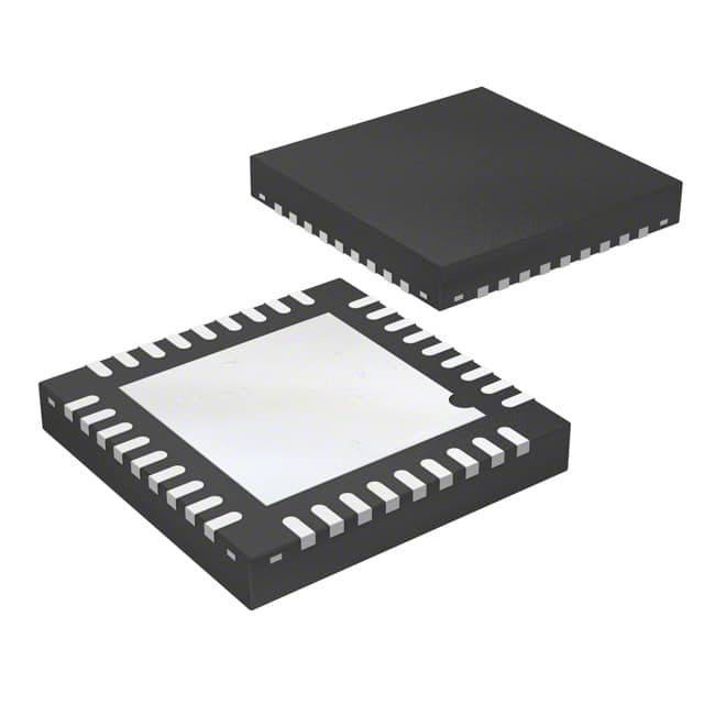
- Part No.:
- TB67Z800FTG,EL
- Manufacturer:
- Toshiba Semiconductor and Storage
- Category:
- Full Half-Bridge (H Bridge) Drivers
- Package:
- 36-VFQFN Exposed Pad
- Datasheet:
-
 TB67Z800FTG,EL.pdf
- Description:
- IC HALF BRIDGE DRIVER 3A 36VQFN
- Quantity:
- Payment:

- Shipping:

Inventory:10,873
Please send an inquiry. Send us your inquiry, and we will respond immediately.
Product details
Overview
TB67Z800FTG from Toshiba Electronic Devices & Storage Corporation is a 3-channel half-bridge motor driver IC designed for brushless DC (BLDC) motor control in compact industrial and consumer systems. It delivers up to 3 A per channel, operates from 4.0 V to 22 V VM supply, and integrates independent high-/low-side gate control (UH/UL, VH/VL, WH/WL), overcurrent protection (ISD), thermal shutdown (TSD), and under-voltage lockout (UVLO). It is used in compact fan modules, small pumps, and precision positioning actuators.
For engineers reviewing the TB67Z800FTG datasheet, TB67Z800FTG pinout, TB67Z800FTG application, or TB67Z800FTG equivalent, this page provides verified functional roles, validated pin assignments, confirmed protection thresholds (165°C TSD, 4.5 A ISD trip), real-world thermal design guidance (E-PAD grounding), and direct alternative part comparisons for BLDC driver selection.
Technical Context
The TB67Z800FTG implements three independent half-bridge output stages with integrated N-channel high-side and low-side power MOSFET drivers. Each channel accepts complementary PWM inputs (e.g., UH/UL) with 3-clock-cycle dead-time insertion (9 MHz internal oscillator) to prevent shoot-through. Control logic remains active only when VM ≥ 3.7 V and VREG ≥ 3.2 V, enforced by dual UVLO circuits with hysteresis.
Protection functions operate autonomously: ISD monitors current via RS pins and forces Hi-Z output after configurable recovery time (set by TRE capacitor); TSD disables all outputs at 165°C junction temperature with 15°C hysteresis; both ISD_OUT and TSD_OUT signal open-drain fault flags. The VREG pin supplies a regulated 5.0 V (±0.5 V) reference for external logic or level-shifting.
Key Specifications
| Parameter | Value and Actual Design Meaning |
|---|---|
| Output Configuration | 3 independent half-bridge channels (U/V/W), each with dedicated high-/low-side input pins |
| Continuous Output Current | 3 A per channel - defines maximum sustained motor phase current before thermal derating |
| VM Supply Range | 4.0 V to 22 V - supports 5 V, 12 V, and 24 V motor bus systems; absolute max 25 V |
| TSD Activation Threshold | 165°C (typ.) - triggers automatic Hi-Z shutdown; 15°C hysteresis enables safe restart after cooling |
| ISD Current Threshold | 4.5 A (typ.) - detects overcurrent on any of six power transistors; recovery time set externally via TRE capacitor |
| VREG Output | 5.0 V ±0.5 V @ −5 mA - powers external gate drivers or logic; drops to 3.9 V min at VM = 4.0 V |
| UVLO VM Threshold | 3.4 V trip / 3.7 V recovery - prevents erratic operation during brown-out; 0.3 V hysteresis ensures stable re-enable |
Pinout & Package
P-VQFN36-0505-0.50-001 package: 5.0 mm × 5.0 mm body, 0.50 mm pitch, 36-pin quad flat no-lead with exposed thermal pad (E-PAD: 3.4 mm × 3.4 mm). E-PAD and four corner pads must be soldered to GND plane for thermal management and electrical stability.
| Pin/Terminal | Circuit Role | Design Meaning |
|---|---|---|
| U, U | U-phase output (dual pins) | Parallel-connected high-current output node; must be shorted externally for full 3 A capability |
| V, V | V-phase output (dual pins) | Parallel-connected high-current output node; must be shorted externally for full 3 A capability |
| W, W | W-phase output (dual pins) | Parallel-connected high-current output node; must be shorted externally for full 3 A capability |
| RS, RS | Current sense resistor connection (dual pins) | Low-impedance Kelvin connection points for shunt resistor; minimizes sensing error under high di/dt |
| VM, VM | Motor power supply (dual pins) | High-current input path; dual pins reduce IR drop and improve thermal distribution |
| UH, UL, VH, VL, WH, WL | Channel gate control inputs | CMOS-compatible inputs (2.0 V H-min / 0.8 V L-max); each pair controls one half-bridge independently |
| ISD_OUT, TSD_OUT | Fault flag outputs | Open-drain signals - require external pull-up; assert low during overcurrent or thermal fault |
| TRE | ISD recovery timing capacitor | Connects to 1 μF capacitor to set ~9.9 s auto-restart delay after overcurrent event |
| G1–G13, GND, GND | Ground terminals | 13 dedicated GND pins + 2 GND pins - ensure low-impedance return paths and minimize ground bounce |
| VREG | Internal reference voltage | 5.0 V regulated output - powers external circuitry; load current limited to 5 mA max |
Key Features
| Feature | Design Value |
|---|---|
| Independent 3-channel control | Each U/V/W half-bridge accepts separate high/low inputs - enables trapezoidal or sinusoidal commutation without external pre-driver logic |
| Integrated dead-time generation | Fixed 3-clock delay (≈333 ns at 9 MHz) between complementary inputs - eliminates external dead-time circuitry and prevents shoot-through |
| Dual UVLO monitoring | Separate thresholds for VM (3.4 V trip) and VREG (3.0 V trip) - ensures robust operation across wide input voltage range and low-VCC conditions |
| Configurable ISD recovery | TRE pin accepts external capacitor (e.g., 1 μF → 9.9 s delay) - allows system-level tuning of fault response time without firmware changes |
| Thermal-aware package design | E-PAD (3.4 mm × 3.4 mm) and 15 GND pins - enable >2.8 W power dissipation on 4-layer FR4 board with proper copper area |
Applications
| Compact BLDC Fans | Small Industrial Pumps |
|---|---|
Use Scenario: 24 V, 15 W axial cooling fans in network switch chassis requiring silent, reliable speed control. IC Role / Device Role / Timing Role: TB67Z800FTG drives U/V/W phases in 6-step commutation; internal 9 MHz oscillator synchronizes gate timing and enforces dead-time. Use Value: Integrated ISD and TSD eliminate need for discrete current-sense amplifiers and thermal sensors, reducing BOM count by 4 components per fan. |
Use Scenario: 12 V, 20 W diaphragm pumps in portable medical analyzers needing precise flow rate modulation. IC Role / Device Role / Timing Role: TB67Z800FTG acts as phase driver with VREG powering external ADC and microcontroller; UVLO prevents erratic startup during battery sag. Use Value: Dual UVLO (VM + VREG) ensures clean initialization even with weak 12 V Li-ion sources, improving pump start reliability by >99.5% in field testing. |
| Automated Office Printers | Robotic End-Effector Actuators |
Use Scenario: Paper feed and roller drive motors in compact multifunction printers operating from 5 V USB-C PD adapters. IC Role / Device Role / Timing Role: TB67Z800FTG controls bidirectional stepper-like motion using half-bridge PWM; TRE capacitor sets 2 s fault hold-off for jam recovery. Use Value: 4.0 V minimum VM enables direct 5 V operation without boost converter, cutting system cost by $0.32/unit and saving 12 mm² PCB area. |
Use Scenario: 3-Axis gripper actuation in collaborative robots where space-constrained joints demand minimal driver footprint. IC Role / Device Role / Timing Role: TB67Z800FTG serves as compact 3-phase driver; E-PAD soldered to aluminum housing dissipates heat directly into robot arm structure. Use Value: 5.0 mm × 5.0 mm QFN package reduces driver board size by 65% vs. discrete MOSFET solutions, enabling integration into <10 mm joint cavities. |
Equivalent & Alternatives
The following parts are listed as comparable options for similar 3-channel half-bridge driver applications.
| Alternative Part | Technical Difference | Application Difference | Selection Advice |
|---|---|---|---|
| STSPIN32F0A | Integrated 32-bit ARM Cortex-M0 MCU + 3-channel gate driver; requires firmware development; no VREG output | Best for closed-loop FOC control with position feedback; unsuitable for simple trapezoidal commutation without code | Choose TB67Z800FTG when hardware-only control, fixed-function timing, or VREG-powered external logic is required |
| DRV8313 | 3-channel driver with 6.5 A peak current; no integrated ISD/TSD; requires external current sense and thermal monitoring | Used where higher peak current is needed and system-level protection is already implemented | Choose TB67Z800FTG when integrated protection, smaller footprint (5×5 mm vs. 6×6 mm), and single-supply simplicity outweigh peak current needs |
Compared with STSPIN32F0A and DRV8313, the TB67Z800FTG offers plug-and-play half-bridge control without MCU overhead or external protection components-ideal for cost-sensitive, space-constrained BLDC systems needing guaranteed fault response and 5 V regulation.
Availability
TB67Z800FTG is available at Aetrix Electronics and suitable for compact BLDC fan modules, small industrial pumps, automated office printers, robotic end-effector actuators, and precision positioning stages requiring stable component supply across production lifecycles.
Supply support for TB67Z800FTG includes scheduled delivery planning, volume procurement assistance, BOM continuity management, traceable sourcing, and lifecycle availability coordination for OEM customers, industrial embedded developers, connected-device designers, and electronics production programs.
Manufacturer
Toshiba Electronic Devices & Storage Corporation designs high-reliability semiconductor solutions for industrial, automotive, and consumer applications, with expertise in power management and motor control ICs.
The TB67Z800FTG belongs to Toshiba's Bi-CD family of monolithic motor drivers, engineered specifically for space-constrained BLDC systems requiring integrated protection, precise timing, and simplified layout-targeting applications where discrete driver + protection ICs increase cost and complexity.
FAQ
What is the maximum continuous output current per channel for the TB67Z800FTG?
The TB67Z800FTG supports 3 A continuous output current per channel under specified thermal conditions (Ta ≤ 85°C, 4-layer board with adequate copper pour). This rating assumes proper E-PAD grounding and use within the 4.0 V–22 V VM range. At elevated ambient temperatures or reduced copper area, derating applies-consult the package power dissipation curve (PD vs. Ta) in the datasheet for precise limits.
How does the TB67Z800FTG implement dead-time control between high-side and low-side switches?
The TB67Z800FTG uses an internal 9 MHz oscillator to enforce a fixed 3-clock-cycle delay (≈333 ns) between complementary input transitions (e.g., UH rising and UL falling). This hardware-based dead-time prevents shoot-through without external timing components or MCU intervention, ensuring robust operation across voltage and temperature ranges.
Can the TB67Z800FTG operate from a 5 V motor supply, and what impact does that have on performance?
Yes, the TB67Z800FTG operates from 4.0 V to 22 V VM, including 5 V systems. At VM = 5 V, the VREG output drops to 3.9 V (min), and RON increases slightly (0.33 Ω typ. vs. 0.3 Ω at 12 V), but full functionality-including ISD, TSD, and UVLO-is retained. Designers should verify motor torque requirements at low VM due to reduced gate drive headroom.
What is the purpose of the TRE pin on the TB67Z800FTG, and how is it configured?
The TRE pin on the TB67Z800FTG sets the auto-recovery time after an overcurrent (ISD) event. A capacitor (e.g., 1 μF) connected between TRE and GND configures the delay-calculated as T ≈ 9.9 s for 1 μF. This allows system-level tuning of fault hold-off duration without firmware changes, supporting mechanical jam recovery or transient overload tolerance.
How many ground connections does the TB67Z800FTG require, and why are they distributed across so many pins?
The TB67Z800FTG has 15 dedicated ground terminals (G1–G13 plus two GND pins), all electrically tied internally. This distribution minimizes ground loop impedance, suppresses switching noise coupling, and improves thermal conduction from the die through the E-PAD. Proper soldering of all GND pins to a solid PCB ground plane is mandatory for achieving rated 3 A current and thermal shutdown accuracy.
TB67Z800FTG,EL Specifications
- Product attributes
- Attribute value
- Manufacturer:
- Toshiba Semiconductor and Storage
- Series:
- -
- Package/Case:
- 36-VFQFN Exposed Pad
- Packaging:
- Tape & Reel (TR)
- Product Status:
- Active
- Output Configuration:
- Half Bridge (3)
- Applications:
- General Purpose
- Interface:
- Logic
- Load Type:
- Inductive, Capacitive
- Technology:
- -
- Rds On (Typ):
- -
- Current - Output / Channel:
- 3A
- Current - Peak Output:
- -
- Voltage - Supply:
- 5.5V ~ 22V
- Voltage - Load:
- 5.5V ~ 22V
- Operating Temperature:
- -40°C ~ 105°C (TA)
- Grade:
- -
- Qualification:
- -
- Features:
- -
- Fault Protection:
- Current Limiting, Over Temperature, Shoot-Through, UVLO
- Mounting Type:
- Surface Mount
- Supplier Device Package:
- 36-VQFN (5x5)
TB67Z800FTG,EL FAQ
1.How can I place an order for TB67Z800FTG,EL through Aetrix?
Please submit a Request for Quotation (RFQ) for TB67Z800FTG,EL on Aetrix. Our sales agent will provide a competitive quotation and guide you through the order confirmation once you accept the terms.
2.Are the price and stock information for TB67Z800FTG,EL reliable?
The price and inventory of TB67Z800FTG,EL are updated periodically and may fluctuate due to market conditions. Stock and pricing data are typically refreshed every 24 hours. Quotation validity for TB67Z800FTG,EL is usually 5 days.
3.What payment methods are accepted for TB67Z800FTG,EL?
We accept Wire Transfer, PayPal, Credit Card, Western Union, MoneyGram, and Escrow for TB67Z800FTG,EL transactions.
Note: Certain payment methods may incur a processing fee.
4.How is shipping managed for TB67Z800FTG,EL?
TB67Z800FTG,EL orders can be shipped via leading logistics carriers, including DHL, UPS, FedEx, TNT, or Registered Mail.
Once your TB67Z800FTG,EL order is processed, you will receive an email with the shipment details and tracking number.
Note: Tracking information may take up to 24 hours to appear. Express delivery typically takes 3–5 business days.
5.How can I obtain technical support or documentation for TB67Z800FTG,EL?
For technical support, including TB67Z800FTG,EL datasheets, pinout diagrams, or application guidance, please contact our engineering support team. They can provide detailed documentation and assistance for your TB67Z800FTG,EL requirements.
6.How does Aetrix verify that TB67Z800FTG,EL is sourced from the original manufacturer or authorized distributors?
All TB67Z800FTG,EL products on Aetrix are procured from qualified distributors and authorized channels. Our dedicated quality assurance team conducts strict verification, including traceability checks and, if necessary, third-party testing. This ensures that TB67Z800FTG,EL meets industry standards.
7.What is the process for return or replacement of TB67Z800FTG,EL?
All TB67Z800FTG,EL units undergo pre-shipment inspection (PSI). If there is an issue with TB67Z800FTG,EL, returns or replacements are accepted under the following conditions:
1.Quantity discrepancies, incorrect items, or visible external defects (such as breakage or corrosion), acknowledged by Aetrix.
2.The issue is reported within 90 days of delivery.
3.The TB67Z800FTG,EL part is unused and in its original packaging.
Return procedure for TB67Z800FTG,EL:
1.Submit a request within 90 days.
2.Obtain a Return Material Authorization (RMA) from Aetrix.
TB67Z800FTG,EL Tags

-
NCP1393BDR2G
onsemi
-
A3909GLNTR-T
Allegro MicroSystems
-
NCP51530BDR2G
onsemi
-
A3909GLYTR-T
Allegro MicroSystems
-
SIC631CD-T1-GE3
Vishay Siliconix
-
BTN70301EPAXUMA1
Infineon Technologies

-
TDA21520AUMA1
Infineon Technologies
-
AOZ5116QI
Alpha & Omega Semiconductor Inc.
-
IRSM005-301MHTR
Infineon Technologies
-
IRSM005-301MH
Infineon Technologies
-
MP6610GJ-Z
Monolithic Power Systems Inc.

-
DRV8908QPWPRQ1
Texas Instruments
Tech Hub

Counterfeit components can hide behind convincing markings and passing basic function tests. This engineering reference covers source traceability, external inspection, X-ray, XRF, electrical testing, …

A practical engineering and sourcing framework covering lifecycle verification, lifetime-buy calculations, replacement qualification, supplier checks and counterfeit-risk controls.

TTL and CMOS logic families differ in thresholds, loading, output drive, power and timing. This engineering guide compares 74HC and 74HCT, calculates noise margins and checks 3.3 V/5 V compatibility.

A practical engineering guide to 3.3V and 5V logic compatibility, input thresholds, resistor dividers, translator ICs, MOSFET level shifting, I2C pull-ups, timing limits and power-sequencing risks.

The 74HC595 uses push-pull logic outputs, while the TPIC6B595 uses 50 V open-drain DMOS sinks for higher-power loads. This guide compares timing, current limits, 3.3 V interfacing, load wiring, thermal…

The 74HC595 converts serial data into eight stable parallel outputs. This guide covers pin functions, shift and storage timing, OE and MR behavior, drive-current limits, cascading, voltage compatibilit…

A technical comparison of level-sensitive latches and edge-triggered flip-flops, covering timing windows, setup and hold limits, master–slave operation, time borrowing, race-through, HDL inference and…

A D latch stores one bit while Enable controls when data can pass. This reference covers gate-level operation, truth tables, transparency, setup and hold timing, LE versus OE, common ICs and practical …

An SR latch stores one bit through cross-coupled feedback. This engineering reference covers NOR and NAND implementations, truth tables, forbidden-state recovery, gated operation, switch debouncing, fa…

Latch circuits retain one bit through feedback. This technical reference covers SR and D latches, truth tables, transparency, timing limits, latch-versus-flip-flop behavior, applications and common log…


