
 My Inquiry
 My Account


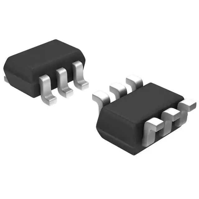
Infineon Technologies BFQ19SH6327XTSA1
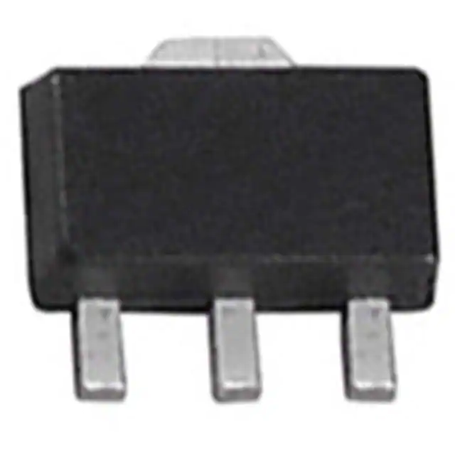
- Part No.:
- BFQ19SH6327XTSA1
- Manufacturer:
- Infineon Technologies
- Category:
- Bipolar RF Transistors
- Package:
- TO-243AA
- Datasheet:
-
 BFQ19SH6327XTSA1.pdf
- Description:
- RF TRANS NPN 15V 5.5GHZ SOT89-3
- Quantity:
- Payment:

- Shipping:

Inventory:2,211
Please send an inquiry. Send us your inquiry, and we will respond immediately.
Product details
Overview
BFQ19SH6327XTSA1 from Infineon Technologies is a low-noise silicon bipolar RF transistor designed for broadband amplifier stages in antenna front-ends and telecom infrastructure up to 1.5 GHz, with fT = 5.5 GHz (typ), NFmin = 1.8 dB at 900 MHz, and P-1dB = 22 dBm at 1.8 GHz. It operates at VCE = 8 V, IC = 70 mA, and delivers Gma = 11.5 dB.
For engineers reviewing the BFQ19SH6327XTSA1 datasheet, BFQ19SH6327XTSA1 pinout, BFQ19SH6327XTSA1 application, or BFQ19SH6327XTSA1 equivalent, key selection criteria include noise figure at 900/1800 MHz, third-order intercept (IP3 = 32 dBm), transducer gain under 50 Ω conditions, and thermal resistance (RthJS = 65 K/W) for RF power stage reliability.
Technical Context
This NPN bipolar RF transistor uses epitaxial base technology optimized for high fT and low noise at collector currents from 10–70 mA. Its SOT89 package enables direct PCB mounting with low-inductance emitter grounding-critical for stable broadband amplification above 500 MHz.
The device supports Class-A operation with VCEO = 15 V and IC = 120 mA absolute maximum ratings. Noise matching (ZSopt) and load matching (ZLopt) are required to achieve NFmin and Gma; SPICE models and S-parameters are available from Infineon's RF model portal.
Key Specifications
| Parameter | Value and Actual Design Meaning |
|---|---|
| fT | 5.5 GHz typical - enables stable gain up to 1.5 GHz with margin for layout parasitics |
| NFmin | 1.8 dB at 900 MHz - critical for cellular LNA sensitivity in GSM/UMTS bands |
| P-1dB | 22 dBm at 1.8 GHz - defines usable linear output power before compression in repeater stages |
| IP3 | 32 dBm at 1.8 GHz - determines intermodulation rejection in multi-carrier base station receivers |
| RthJS | 65 K/W - sets thermal derating slope for continuous-wave operation on FR4 PCBs |
| Ccb | 1.05 pF typical - limits Miller effect and stabilizes high-frequency feedback design |
| hFE | 70–140 at IC = 70 mA - ensures consistent bias point across production lots |
Pinout & Package
SOT89 package: surface-mount, 3-pin, thermally enhanced plastic case with exposed collector tab soldered directly to PCB ground plane for low RthJS.
| Pin/Terminal | Circuit Role | Design Meaning |
|---|---|---|
| 1 (Tab) | Collector | Exposed metal tab - must be soldered to large copper pour for thermal conduction and RF grounding |
| 2 | Base | High-impedance control node - requires DC blocking and impedance-matching network for RF drive |
| 3 | Emitter | Low-impedance current return - grounded via shortest possible path to minimize inductive reactance above 500 MHz |
Key Features
| Feature | Design Value |
|---|---|
| Low minimum noise figure | NFmin = 1.8 dB at 900 MHz - enables receiver sensitivity down to –115 dBm in 200 kHz bandwidth |
| High transition frequency | fT = 5.5 GHz - supports stable small-signal gain in UMTS Band I (1920–1980 MHz) and LTE Band 3 (1710–1785 MHz) |
| Robust linearity | IP3 = 32 dBm and P-1dB = 22 dBm - allows simultaneous amplification of multiple carriers without adjacent-channel interference |
| AEC-Q101 qualified | Qualified per automotive stress test standard - validated for use in harsh-environment telecom outdoor units and remote radio heads |
| RoHS-compliant packaging | Pb-free SOT89 - meets EU Directive 2011/65/EU and supports lead-free reflow assembly |
Applications
| Cellular Base Station LNA | GSM/UMTS Antenna Tuner Driver |
|---|---|
Use Scenario: Low-noise amplification of weak signals received by sector antennas in macrocell BTS. IC Role / Device Role / Timing Role: First-stage NPN RF transistor in cascode configuration with matched input impedance. Use Value: Achieves system noise figure < 2.0 dB at 900 MHz using ZSopt matching, enabling 3GPP-compliant sensitivity. | Use Scenario: Driving tunable matching networks in adaptive antenna systems for multi-band handsets. IC Role / Device Role / Timing Role: High-linearity driver stage delivering 22 dBm P-1dB into variable capacitive loads. Use Value: Maintains IP3 > 30 dBm across 800–2200 MHz, ensuring harmonic suppression in envelope-tracking PA modules. |
| Repeaters and Small Cells | ISM Band 915 MHz Transceivers |
Use Scenario: Bidirectional amplification in in-building femtocell repeaters operating at 1800/1900 MHz. IC Role / Device Role / Timing Role: Dual-purpose RF transistor used in both receive LNA and transmit driver paths. Use Value: Enables single-component reuse across signal chains, reducing BOM count and calibration complexity. | Use Scenario: Receiver front-end in industrial IoT gateways compliant with FCC Part 15.247. IC Role / Device Role / Timing Role: Low-noise active device in discrete LNA with external 50 Ω input match. Use Value: Delivers NF < 2.2 dB and gain > 10 dB at 915 MHz, meeting link budget requirements for 100 m range LoRaWAN nodes. |
Equivalent & Alternatives
The following parts are listed as comparable options for similar low-noise RF transistor applications.
| Alternative Part | Technical Difference | Application Difference | Selection Advice |
|---|---|---|---|
| BFP180H6327XTSA1 | fT = 7 GHz, NFmin = 1.3 dB at 900 MHz, RthJS = 55 K/W, SOT343 package | Higher gain and lower noise but smaller package limits power handling (P-1dB = 18 dBm) | Select for ultra-low-noise LNA where thermal headroom exceeds 1 W dissipation requirement |
| MRF5812LSR3 | fT = 4.5 GHz, NFmin = 2.0 dB at 900 MHz, TO-247 package, higher P-1dB (25 dBm) | Through-hole mounting, higher thermal mass, not RoHS-compliant | Select for legacy industrial amplifiers requiring mechanical robustness over surface-mount density |
Compared with BFP180H6327XTSA1, BFQ19SH6327XTSA1 trades 0.5 dB NFmin for +4 dBm P-1dB and 10 K/W higher thermal resistance-making it preferable for medium-power repeater stages. Against MRF5812LSR3, it offers RoHS compliance and SMT compatibility at the cost of lower ruggedness in vibration-prone deployments.
Availability
BFQ19SH6327XTSA1 is available at Aetrix Electronics and suitable for cellular base station LNAs, repeater RF front-ends, and ISM band transceiver designs requiring stable component supply across multi-year production cycles.
Supply support for BFQ19SH6327XTSA1 includes scheduled delivery planning, volume procurement assistance, BOM continuity management, traceable sourcing, and lifecycle availability coordination for OEM customers, industrial embedded developers, connected-device designers, and electronics production programs.
Manufacturer
Infineon Technologies AG is a German semiconductor manufacturer specializing in power management, RF, automotive, and security ICs, with global manufacturing and R&D centers.
The BFQ19S series belongs to Infineon's discrete RF transistor product line, engineered specifically for high-linearity, low-noise amplification in wireless infrastructure equipment operating below 2 GHz.
FAQ
What is the recommended bias condition for optimal noise figure at 900 MHz?
For NFmin = 1.8 dB at 900 MHz, operate at VCE = 6 V and IC = 20 mA with source impedance ZS = ZSopt = 12 + j15 Ω. This condition is verified in the datasheet's AC characteristics table and requires external matching network implementation-not internal circuitry.
Can BFQ19SH6327XTSA1 be used in Class AB amplifier configurations?
Yes, it supports Class AB operation with proper base biasing and emitter degeneration. The hFE range (70–140) and fT stability allow predictable gain compression behavior, but thermal design must account for RthJS = 65 K/W under pulsed or modulated RF loads per the derating curve in datasheet Figure 4.
Is the SOT89 package lead-free and compatible with standard Pb-free reflow profiles?
Yes, BFQ19SH6327XTSA1 is RoHS-compliant with Pb-free terminations and rated for JEDEC J-STD-020D-compliant reflow. Peak temperature must not exceed 260 °C for ≤ 30 seconds; the exposed collector tab requires full wetting during soldering to ensure thermal performance.
Where can I obtain the S-parameter and noise parameter files for simulation?
S-parameters (including noise parameters) and SPICE GP models are hosted on Infineon's official RF model portal at www.infineon.com/rf.models. Users must download the latest version directly from that site-no embedded models are included in the datasheet PDF.
BFQ19SH6327XTSA1 Specifications
- Product attributes
- Attribute value
- Manufacturer:
- Infineon Technologies
- Series:
- -
- Package/Case:
- TO-243AA
- Packaging:
- Tape & Reel (TR)
- Product Status:
- Active
- Transistor Type:
- NPN
- Voltage - Collector Emitter Breakdown (Max):
- 15V
- Frequency - Transition:
- 5.5GHz
- Noise Figure (dB Typ @ f):
- 3dB @ 1.8GHz
- Gain:
- 7dB
- Power - Max:
- 1W
- DC Current Gain (hFE) (Min) @ Ic, Vce:
- 70 @ 70mA, 8V
- Current - Collector (Ic) (Max):
- 120mA
- Operating Temperature:
- 150°C (TJ)
- Grade:
- -
- Qualification:
- -
- Mounting Type:
- Surface Mount
- Supplier Device Package:
- PG-SOT89
BFQ19SH6327XTSA1 FAQ
1.How can I place an order for BFQ19SH6327XTSA1 through Aetrix?
Please submit a Request for Quotation (RFQ) for BFQ19SH6327XTSA1 on Aetrix. Our sales agent will provide a competitive quotation and guide you through the order confirmation once you accept the terms.
2.Are the price and stock information for BFQ19SH6327XTSA1 reliable?
The price and inventory of BFQ19SH6327XTSA1 are updated periodically and may fluctuate due to market conditions. Stock and pricing data are typically refreshed every 24 hours. Quotation validity for BFQ19SH6327XTSA1 is usually 5 days.
3.What payment methods are accepted for BFQ19SH6327XTSA1?
We accept Wire Transfer, PayPal, Credit Card, Western Union, MoneyGram, and Escrow for BFQ19SH6327XTSA1 transactions.
Note: Certain payment methods may incur a processing fee.
4.How is shipping managed for BFQ19SH6327XTSA1?
BFQ19SH6327XTSA1 orders can be shipped via leading logistics carriers, including DHL, UPS, FedEx, TNT, or Registered Mail.
Once your BFQ19SH6327XTSA1 order is processed, you will receive an email with the shipment details and tracking number.
Note: Tracking information may take up to 24 hours to appear. Express delivery typically takes 3–5 business days.
5.How can I obtain technical support or documentation for BFQ19SH6327XTSA1?
For technical support, including BFQ19SH6327XTSA1 datasheets, pinout diagrams, or application guidance, please contact our engineering support team. They can provide detailed documentation and assistance for your BFQ19SH6327XTSA1 requirements.
6.How does Aetrix verify that BFQ19SH6327XTSA1 is sourced from the original manufacturer or authorized distributors?
All BFQ19SH6327XTSA1 products on Aetrix are procured from qualified distributors and authorized channels. Our dedicated quality assurance team conducts strict verification, including traceability checks and, if necessary, third-party testing. This ensures that BFQ19SH6327XTSA1 meets industry standards.
7.What is the process for return or replacement of BFQ19SH6327XTSA1?
All BFQ19SH6327XTSA1 units undergo pre-shipment inspection (PSI). If there is an issue with BFQ19SH6327XTSA1, returns or replacements are accepted under the following conditions:
1.Quantity discrepancies, incorrect items, or visible external defects (such as breakage or corrosion), acknowledged by Aetrix.
2.The issue is reported within 90 days of delivery.
3.The BFQ19SH6327XTSA1 part is unused and in its original packaging.
Return procedure for BFQ19SH6327XTSA1:
1.Submit a request within 90 days.
2.Obtain a Return Material Authorization (RMA) from Aetrix.
BFQ19SH6327XTSA1 Tags
-
BFR182WH6327XTSA1
Infineon Technologies
-
BFR92PE6327HTSA1
Infineon Technologies
-
BFR360FH6327XTSA1
Infineon Technologies
-
BFR193FH6327XTSA1
Infineon Technologies
-
BFU550AR
NXP USA Inc.
-
BFR460L3E6327XTMA1
Infineon Technologies
-
MMBTH81
onsemi
-
BFU520WX
NXP USA Inc.
-
BFP840FESDH6327XTSA1
Infineon Technologies
-
BFP650H6327XTSA1
Infineon Technologies
-
BFU520AR
NXP USA Inc.
-
BFS483H6327XTSA1
Infineon Technologies
Tech Hub

Jumper cables guide covering safe connection order, red and black clamp placement, final ground connection, cable gauge, length, clamp quality, copper vs CCA cables, jump starter comparison and battery…

LDO regulator guide covering low dropout voltage, power dissipation, thermal design, PSRR, output noise, capacitor stability, adjustable LDO circuits, LDO vs buck converter and datasheet selection chec…

Conditional Access Module guide covering CAM meaning, CI/CI+ interface, smart card authorization, DVB security workflow, TV and set-top box compatibility, internal electronics, ESD protection, connecto…

Guide to electronic component obsolescence covering EOL risk, PCN/PDN notices, last-time buy planning, replacement options, form-fit-function validation, counterfeit risk and BOM lifecycle management.

18650 battery guide covering lithium-ion cell basics, 3.6V/3.7V voltage, 4.2V charging, mAh and Wh capacity, protected cells, chargers, BMS, series-parallel packs, holders, welding and sourcing checks.…

Hall effect sensor guide covering working principle, linear and digital sensors, Arduino circuits, current sensing, speed detection, automotive applications, A3144 examples, signal filtering and datash…

Product Change Notification guide for electronic components, covering PCN meaning, PCN vs PDN/EOL, common change types, risk levels, form-fit-function review, engineering validation, BOM control, LTB/L…

A practical guide to blend door actuators, covering HVAC function, symptoms, location, AC and heater issues, reset and calibration, replacement cost, electrical diagnosis, compatibility checks, and rep…

Engineering guide to Raspberry Pi alternatives, covering chip-level differences, Orange Pi, ROCK, Jetson, Banana Pi, NanoPi, Compute Module, Pico, GPIO, camera, HAT compatibility, and replacement risks…

Engineering guide to dynamic load response testing for high-current buck converters, covering load step setup, slew rate, Vcore undershoot, overshoot, recovery time, probe location, output capacitors a…


