
 My Inquiry
 My Account


NXP Semiconductors BLS3135-10,114
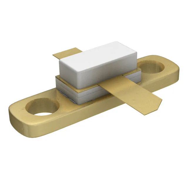
- Part No.:
- BLS3135-10,114
- Manufacturer:
- NXP Semiconductors
- Category:
- Bipolar RF Transistors
- Package:
- SOT-445C
- Datasheet:
-
 BLS3135-10,114.pdf
- Description:
- RF TRANS NPN 75V 3.5GHZ CDFM2
- Quantity:
- Payment:

- Shipping:

Inventory:6,786
Please send an inquiry. Send us your inquiry, and we will respond immediately.
Product details
Overview
BLS3135-10 from Philips Semiconductors is an NPN silicon planar epitaxial microwave power transistor in SOT445C flanged ceramic package, designed for common-base class-C pulsed operation at 3.1–3.5 GHz. It delivers ≥10 W RF output power with ≥7.5 dB power gain and typical 40% collector efficiency at VCB = 40 V, tp = 100 µs, δ = 10%, and is optimized for radar transmitter stages.
For engineers reviewing the BLS3135-10 datasheet, BLS3135-10 pinout, BLS3135-10 application, or BLS3135-10 equivalent, this device requires attention to thermal impedance (5.2 K/W), BeO-based heatsink interface safety, base-to-flange grounding, and pulse-duty-cycle–dependent derating in high-reliability radar systems.
Technical Context
The BLS3135-10 employs an interdigitated emitter-base structure and multicell geometry to enhance emitter efficiency and reduce thermal resistance. Its internal input/output matching networks simplify integration into 3.1–3.5 GHz pulsed amplifier designs without external tuning components.
It operates exclusively in common-base configuration with the base internally connected to the flange - a fixed, low-inductance ground reference. Emitter ballasting resistors and gold metallization are integrated to ensure ruggedness and long-term reliability under repetitive high-peak-current pulsing.
Key Specifications
| Parameter | Value and Actual Design Meaning |
|---|---|
| RF Frequency Range | 3.1–3.5 GHz - supports X-band radar pulse amplification with stable gain and efficiency across full band |
| Output Power (PL) | ≥10 W - minimum guaranteed pulsed RF power at 10% duty cycle, enabling medium-range radar transmit stages |
| Power Gain (Gp) | ≥7.5 dB - sufficient drive margin for cascaded radar PA stages without intermediate amplification |
| Collector Efficiency (ηC) | Typ. 40% - reduces heat generation per watt of RF output, easing thermal management in compact radar modules |
| Thermal Impedance (Zth j-h) | 5.2 K/W @ tp = 100 µs - defines heatsink requirement for junction temperature control under pulsed operation |
| Breakdown Voltage (V(BR)CBO) | 75 V - enables safe operation at 40 V collector-base bias with 87.5% voltage headroom against avalanche |
| Peak Collector Current (ICM) | 1.5 A - supports high instantaneous current during short pulses without second-breakdown risk |
Pinout & Package
SOT445C is a hermetic, flanged ceramic package with two leads and base-to-flange connection. The rectangular copper flange provides mechanical mounting, RF grounding, and primary thermal path to heatsink. Ceramic cap isolates internal die; beryllium oxide (BeO) substrate ensures high thermal conductivity but mandates handling precautions.
| Pin/Terminal | Circuit Role | Design Meaning |
|---|---|---|
| 1 | Collector | Main RF power output node; requires low-inductance connection to output matching network and heatsink isolation |
| 2 | Emiter | RF input node in common-base configuration; connects to driver stage via broadband matching network |
| 3 | Base (flange-connected) | DC and RF ground reference; must be bolted directly to grounded heatsink with conductive thermal interface material |
Key Features
| Feature | Design Value |
|---|---|
| Internal input/output matching | Eliminates need for external tuning stubs or lumped LC networks in 3.1–3.5 GHz band, reducing board area and assembly steps |
| Emitter ballasting resistors | Prevents current hogging across multicell emitters during pulse transients, improving pulse-to-pulse consistency and lifetime |
| Gold metallization | Ensures bond-wire reliability and corrosion resistance over >10-year field deployment in humid or thermally cycled environments |
| Interdigitated emitter-base structure | Increases emitter injection efficiency and reduces base spreading resistance, supporting higher fT and gain at X-band |
| Multicell geometry | Distributes power dissipation across parallel transistor cells, lowering local junction temperature and thermal stress gradients |
Applications
| Ground-Based Radar Transmitter | Airborne Pulse Doppler Radar |
|---|---|
|
Use Scenario: Medium-range surveillance radar operating at 3.3 GHz with 100 µs pulse width and 10% duty cycle. IC Role / Device Role / Timing Role: Final-stage pulsed RF power amplifier in common-base configuration, driven by pre-driver stage. Use Value: Delivers ≥10 W saturated output with 40% efficiency, minimizing DC power draw and heatsink mass in mobile radar platforms. |
Use Scenario: Airborne weather radar requiring rugged, lightweight X-band PA with high pulse-to-pulse repeatability. IC Role / Device Role / Timing Role: High-reliability pulsed power transistor mounted on aluminum heatsink with BeO thermal interface. Use Value: Emitter ballasting and gold metallization maintain performance stability across wide temperature (-40°C to +85°C ambient) and vibration profiles. |
| Maritime Navigation Radar | Electronic Warfare Jammer Module |
|
Use Scenario: Coastal vessel navigation radar operating in humid salt-laden environment with frequent on/off cycling. IC Role / Device Role / Timing Role: Class-C pulsed amplifier in transmit chain, leveraging internal matching for rapid deployment and minimal tuning. Use Value: Ceramic hermetic package and gold interconnects prevent moisture-induced degradation and contact corrosion over 15+ year service life. |
Use Scenario: Compact EW pod requiring high peak power density and fast pulse response in 3.1–3.5 GHz band. IC Role / Device Role / Timing Role: Medium-power RF switch-amplifier element in solid-state jammer front-end, gated at microsecond intervals. Use Value: Low Zth j-h (5.2 K/W) and multicell layout enable high peak power bursts without thermal runaway during burst-mode operation. |
Equivalent & Alternatives
The following parts are listed as comparable options for similar microwave pulsed power amplifier applications.
| Alternative Part | Technical Difference | Application Difference | Selection Advice |
|---|---|---|---|
| MRF377 | Higher PL (25 W), wider bandwidth (2.7–3.1 GHz), TO-247 package with isolated collector | Requires external matching; better suited for lower-frequency radar with higher power demand and less stringent size constraints | Select when ≥20 W output and broader bandwidth are required, and PCB space allows larger TO-247 footprint |
| BLF278 | Limited to 2.7–2.9 GHz, 12 W PL, same SOT445C package but no BeO - lower thermal impedance (4.5 K/W) but reduced frequency coverage | Optimized for legacy L-band radar upgrades; lacks 3.1–3.5 GHz support needed for modern X-band systems | Select only for retrofit applications below 3.0 GHz where existing layout and thermal design match SOT445C footprint |
Compared with MRF377 and BLF278, the BLS3135-10 uniquely balances 3.1–3.5 GHz coverage, ≥10 W output, and SOT445C form factor - making it the only option among the three qualified for compact, frequency-specific X-band radar transmitters requiring internal matching and flange-grounded base topology.
Availability
BLS3135-10 is available at Aetrix Electronics and suitable for ground-based radar transmitters, airborne pulse Doppler systems, and maritime navigation radars requiring stable component supply, controlled thermal interface sourcing, and compliance with legacy military-grade microwave transistor specifications.
Supply support for BLS3135-10 includes scheduled delivery planning, volume procurement assistance, BOM continuity management, traceable sourcing, and lifecycle availability coordination for OEM customers, industrial embedded developers, connected-device designers, and electronics production programs.
Manufacturer
Philips Semiconductors (now NXP Semiconductors) is a global leader in high-frequency discrete semiconductors, with expertise in RF power devices for defense and aerospace applications.
The BLS3135-10 belongs to Philips' microwave power transistor family engineered specifically for ruggedized, high-efficiency pulsed amplification in X-band radar systems - emphasizing thermal robustness, internal matching, and flange-grounded reliability.
FAQ
What is the maximum allowable junction temperature for the BLS3135-10?
The BLS3135-10 has a maximum operating junction temperature (Tj) of 200 °C, as specified in its limiting values table. This rating assumes proper heatsinking and adherence to pulsed operating conditions (tp ≤ 100 µs, δ ≤ 10%). Exceeding this temperature risks permanent degradation of the BeO substrate and gold metallization integrity. Thermal design must ensure Tj remains within limit using Zth j-h = 5.2 K/W and ambient/heatsink temperature data.
Why is the base terminal connected to the flange in the BLS3135-10?
The base terminal of the BLS3135-10 is permanently bonded to the metal flange to establish a low-inductance, low-impedance RF ground reference essential for stable common-base operation at 3.1–3.5 GHz. This eliminates base lead inductance that would otherwise degrade gain and cause instability. Mounting the flange directly to a grounded heatsink ensures optimal RF return path and thermal conduction - a non-negotiable requirement confirmed in the device's pinning diagram and application circuit layout.
Does the BLS3135-10 require external matching networks?
No - the BLS3135-10 integrates internal input and output matching networks optimized for 3.1–3.5 GHz operation in common-base class-C mode, as stated in its Features section and verified in Fig.8 test circuit layout. External matching is unnecessary for nominal operation; however, fine-tuning may be applied for specific load impedances or harmonic suppression. The internal matching enables simplified PCB layout and repeatable performance across production units without manual tuning.
What safety precautions apply when handling the BLS3135-10?
The BLS3135-10 contains beryllium oxide (BeO) in its ceramic package substrate. If the BeO disc is damaged - e.g., by mechanical impact, improper soldering, or flange bending - toxic beryllium particles may be released. Users must avoid grinding, drilling, or breaking the package; dispose of failed units as chemical/special waste per local regulations; and never discard with general waste. Full safety guidance is provided in the datasheet's WARNING section on page 3.
Can the BLS3135-10 be used in continuous-wave (CW) mode?
No - the BLS3135-10 is characterized and rated exclusively for pulsed operation (tp ≤ 100 µs, δ ≤ 10%). Its thermal characteristics (e.g., Zth j-h = 5.2 K/W) and limiting values (Ptot = 34 W only at pulsed conditions) do not support sustained CW dissipation. Attempting CW operation risks immediate thermal runaway and junction failure. All published RF performance data - including Gp, ηC, and PL - assume strict adherence to pulsed test conditions defined in the Quick Reference Data table.
BLS3135-10,114 Specifications
- Product attributes
- Attribute value
- Manufacturer:
- NXP Semiconductors
- Series:
- -
- Package/Case:
- SOT-445C
- Packaging:
- Tray
- Product Status:
- Obsolete
- Transistor Type:
- NPN
- Voltage - Collector Emitter Breakdown (Max):
- 75V
- Frequency - Transition:
- 3.5GHz
- Noise Figure (dB Typ @ f):
- -
- Gain:
- 9dB
- Power - Max:
- 34W
- DC Current Gain (hFE) (Min) @ Ic, Vce:
- 40 @ 250mA, 5V
- Current - Collector (Ic) (Max):
- 1.5A
- Operating Temperature:
- 200°C (TJ)
- Grade:
- -
- Qualification:
- -
- Mounting Type:
- Chassis Mount
- Supplier Device Package:
- CDFM2
BLS3135-10,114 FAQ
1.How can I place an order for BLS3135-10,114 through Aetrix?
Please submit a Request for Quotation (RFQ) for BLS3135-10,114 on Aetrix. Our sales agent will provide a competitive quotation and guide you through the order confirmation once you accept the terms.
2.Are the price and stock information for BLS3135-10,114 reliable?
The price and inventory of BLS3135-10,114 are updated periodically and may fluctuate due to market conditions. Stock and pricing data are typically refreshed every 24 hours. Quotation validity for BLS3135-10,114 is usually 5 days.
3.What payment methods are accepted for BLS3135-10,114?
We accept Wire Transfer, PayPal, Credit Card, Western Union, MoneyGram, and Escrow for BLS3135-10,114 transactions.
Note: Certain payment methods may incur a processing fee.
4.How is shipping managed for BLS3135-10,114?
BLS3135-10,114 orders can be shipped via leading logistics carriers, including DHL, UPS, FedEx, TNT, or Registered Mail.
Once your BLS3135-10,114 order is processed, you will receive an email with the shipment details and tracking number.
Note: Tracking information may take up to 24 hours to appear. Express delivery typically takes 3–5 business days.
5.How can I obtain technical support or documentation for BLS3135-10,114?
For technical support, including BLS3135-10,114 datasheets, pinout diagrams, or application guidance, please contact our engineering support team. They can provide detailed documentation and assistance for your BLS3135-10,114 requirements.
6.How does Aetrix verify that BLS3135-10,114 is sourced from the original manufacturer or authorized distributors?
All BLS3135-10,114 products on Aetrix are procured from qualified distributors and authorized channels. Our dedicated quality assurance team conducts strict verification, including traceability checks and, if necessary, third-party testing. This ensures that BLS3135-10,114 meets industry standards.
7.What is the process for return or replacement of BLS3135-10,114?
All BLS3135-10,114 units undergo pre-shipment inspection (PSI). If there is an issue with BLS3135-10,114, returns or replacements are accepted under the following conditions:
1.Quantity discrepancies, incorrect items, or visible external defects (such as breakage or corrosion), acknowledged by Aetrix.
2.The issue is reported within 90 days of delivery.
3.The BLS3135-10,114 part is unused and in its original packaging.
Return procedure for BLS3135-10,114:
1.Submit a request within 90 days.
2.Obtain a Return Material Authorization (RMA) from Aetrix.
BLS3135-10,114 Tags
-
BFR182WH6327XTSA1
Infineon Technologies
-
BFR92PE6327HTSA1
Infineon Technologies
-
BFR360FH6327XTSA1
Infineon Technologies
-
BFR193FH6327XTSA1
Infineon Technologies
-
BFU550AR
NXP USA Inc.
-
BFR460L3E6327XTMA1
Infineon Technologies
-
MMBTH81
onsemi
-
BFU520WX
NXP Semiconductors
-
BFP840FESDH6327XTSA1
Infineon Technologies
-
BFP650H6327XTSA1
Infineon Technologies
-
BFU520AR
NXP Semiconductors
-
BFS483H6327XTSA1
Infineon Technologies
Tech Hub

A practical engineering guide to 3.3V and 5V logic compatibility, input thresholds, resistor dividers, translator ICs, MOSFET level shifting, I2C pull-ups, timing limits and power-sequencing risks.

The 74HC595 uses push-pull logic outputs, while the TPIC6B595 uses 50 V open-drain DMOS sinks for higher-power loads. This guide compares timing, current limits, 3.3 V interfacing, load wiring, thermal…

The 74HC595 converts serial data into eight stable parallel outputs. This guide covers pin functions, shift and storage timing, OE and MR behavior, drive-current limits, cascading, voltage compatibilit…

A technical comparison of level-sensitive latches and edge-triggered flip-flops, covering timing windows, setup and hold limits, master–slave operation, time borrowing, race-through, HDL inference and…

A D latch stores one bit while Enable controls when data can pass. This reference covers gate-level operation, truth tables, transparency, setup and hold timing, LE versus OE, common ICs and practical …

An SR latch stores one bit through cross-coupled feedback. This engineering reference covers NOR and NAND implementations, truth tables, forbidden-state recovery, gated operation, switch debouncing, fa…

Latch circuits retain one bit through feedback. This technical reference covers SR and D latches, truth tables, transparency, timing limits, latch-versus-flip-flop behavior, applications and common log…

An engineering guide to LED driver operation, constant-current and constant-voltage outputs, linear and switching topologies, dimming, IC selection, calculations, replacement compatibility, and fault c…

Operational amplifier guide covering op amp basics, feedback, ideal vs real op amps, common configurations, buffer circuits, offset, bias current, gain-bandwidth, slew rate, rail-to-rail limits and sel…

Jumper cables guide covering safe connection order, red and black clamp placement, final ground connection, cable gauge, length, clamp quality, copper vs CCA cables, jump starter comparison and battery…


